Light emitting diode epitaxial wafer and fabrication method thereof

A technology of light-emitting diodes and manufacturing methods, which is applied in the direction of electrical components, circuits, semiconductor devices, etc., and can solve problems such as inability to merge and offset dislocations and defects, damage, and reduction in the growth quality of epitaxial wafers

Active Publication Date: 2017-12-08
HC SEMITEK ZHEJIANG CO LTD
View PDF5 Cites 10 Cited by
  • Summary
  • Abstract
  • Description
  • Claims
  • Application Information

AI Technical Summary

Problems solved by technology

[0006] If PSS is used on the substrate, and an AlN buffer layer is set between the substrate and the GaN material, the GaN material is very weak on the AlN buffer layer because the enablement of the AlN surface is lower than that of sapphire. Easy to grow, the characteristics of gallium nitride material on the tapered slope of PSS to select the direction for lateral growth will be destroyed, unable to merge and offset the dislocations and defects caused by the lattice mismatch between gallium nitride material and sapphire, and the growth of epitaxial wafers quality will decrease

Method used


Image

  • Light emitting diode epitaxial wafer and fabrication method thereof
  • Light emitting diode epitaxial wafer and fabrication method thereof
  • Light emitting diode epitaxial wafer and fabrication method thereof

Examples


Embodiment 1

[0043] An embodiment of the present invention provides a method for manufacturing a light-emitting diode epitaxial wafer, see figure 1 , the production method includes:

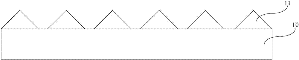
[0044] Step 101: Provide a patterned sapphire substrate, one surface of the patterned sapphire substrate is provided with patterns arranged periodically.

[0045] Figure 2a It is a schematic structural diagram of the epitaxial wafer after step 101 is executed. Wherein, 10 represents a patterned sapphire substrate, and 11 represents a pattern. Such as Figure 2a As shown, several patterns 11 are arranged at equal intervals on one surface of the patterned sapphire substrate 10 .

[0046] Optionally, the maximum distance between two points on the bottom surface of a figure may be equal to the distance between two adjacent figures.

[0047] Wherein, the bottom surface of the figure is the surface in contact with the patterned sapphire substrate, and the maximum distance between two points on the bottom surf...

Embodiment 2

[0111] An embodiment of the present invention provides a method for manufacturing a light-emitting diode epitaxial wafer, and the method provided in this embodiment is a specific implementation of the method provided in Embodiment 2. see image 3 , the production method includes:

[0112] Step 201: Provide a patterned sapphire substrate, one surface of the patterned sapphire substrate is provided with patterns arranged periodically, the period of the patterns is 3 μm, and the height of the patterns is 1.6 μm.

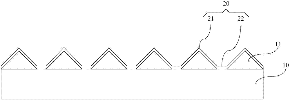
[0113] Step 202: forming an aluminum nitride buffer layer with a thickness of 300 nm on the surface of the patterned sapphire substrate provided with patterns, the aluminum nitride buffer layer including a first part on the pattern and a second part between the patterns.

[0114] Step 203: Coating photoresist on the aluminum nitride buffer layer, the thickness of the photoresist on the first part is smaller than the thickness of the photoresist on the second part, the ...

Embodiment 3

[0122] An embodiment of the present invention provides a light-emitting diode epitaxial wafer. The epitaxial wafer provided in this embodiment can be manufactured by the manufacturing method provided in Embodiment 1 or Embodiment 2. Refer to Figure 4 , the light-emitting diode epitaxial wafer includes a patterned sapphire substrate 10, an aluminum nitride buffer layer 20, a silicon dioxide layered structure 30, an N-type gallium nitride layer 40, a light-emitting layer 50, and a P-type gallium nitride layer 60. One surface of the patterned sapphire substrate 10 is provided with periodically arranged patterns 11, the silicon dioxide layered structure 30 is arranged on the top of each pattern 11, and the aluminum nitride buffer layer 20 is arranged on the top of the patterned sapphire substrate 10 except the pattern 11 In the area other than the N-type gallium nitride layer 40 is arranged on the aluminum nitride buffer layer 20 and the silicon dioxide layered structure 30, the l...


PUM

PropertyMeasurementUnit
thicknessaaaaaaaaaa
thicknessaaaaaaaaaa
thicknessaaaaaaaaaa

Abstract

The invention discloses a light emitting diode epitaxial wafer and a fabrication method thereof, and belongs to the technical field of semiconductors. The fabrication method comprises the steps of providing a patterned sapphire substrate (PSS); forming an aluminum nitride buffer layer on a surface, on which patterns are arranged, of the PPS, wherein the aluminum nitride buffer layer comprises first parts and second parts, the first parts are arranged on the patterns, the second parts are arranged among the patterns; coating photoresist on the aluminum nitride buffer layer, wherein the thickness of the photoresist arranged on the first parts is smaller than the thickness of the photoresist arranged on the second parts; performing dry etching on the photoresist until the photoresist arranged at the tops of the first parts is removed; removing the tops of the first parts; laying a silicon dioxide material; removing the residual photoresist to form a silicon dioxide layered structure; and sequentially growing an N-type gallium nitride layer, a light emitting layer and a P-type gallium nitride layer. By the fabrication method, the epitaxial defect of a top end of the PPS caused by the aluminum nitride buffer layer can be prevented, and lattice mismatching also can be buffered by the aluminum nitride buffer layer.

Description

technical field [0001] The invention relates to the technical field of semiconductors, in particular to a light-emitting diode epitaxial wafer and a manufacturing method thereof. Background technique [0002] A light emitting diode (English: Light Emitting Diode, referred to as: LED) is a semiconductor device that can convert electrical energy into light energy. The chip is the core component of the LED, and the chip includes an epitaxial wafer and electrodes arranged on the epitaxial wafer. [0003] The existing epitaxial wafer includes a substrate and an N-type semiconductor layer, a light-emitting layer and a P-type semiconductor layer stacked on the substrate in sequence. Wherein, the substrate is made of sapphire, and the N-type semiconductor layer, light emitting layer and P-type semiconductor layer are made of gallium nitride (GaN) material. [0004] There is a large lattice mismatch between GaN material and sapphire. In order to alleviate the lattice mismatch betw...

Claims


Application Information

Patent Timeline
Patent Type & Authority Applications(China)
IPC IPC(8): H01L33/00H01L33/06H01L33/12
CPCH01L33/0075H01L33/06H01L33/12
Inventor 尹灵峰王江波
Owner HC SEMITEK ZHEJIANG CO LTD
Why Eureka
Try Eureka