Display substrate and preparing method thereof and display device

A technology of display substrate and display structure, applied in the direction of identification devices, instruments, etc., can solve the problems of low bonding yield and uneven stress, and achieve the effect of avoiding the phenomenon of IC short circuit

Active Publication Date: 2017-12-12
BOE TECH GRP CO LTD
View PDF7 Cites 14 Cited by
  • Summary
  • Abstract
  • Description
  • Claims
  • Application Information

AI Technical Summary

Problems solved by technology

[0005] The technical problem to be solved by the present invention is to provide a display substrate, a method for preparing a display substrate, and a display device for the above-mentioned deficiencies in the prior art, at least partly solving the stress instability caused by the COP bonding process of the IC chip in the flexible display structure. Average, low bonding yield

Method used


Image

  • Display substrate and preparing method thereof and display device
  • Display substrate and preparing method thereof and display device
  • Display substrate and preparing method thereof and display device

Examples


Embodiment 1

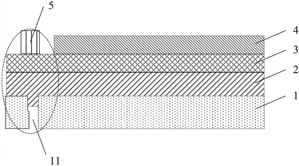
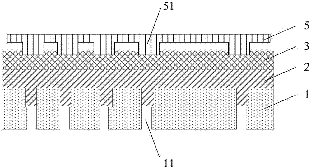
[0027] Aiming at the problem that the IC is directly crimped on the flexible display structure in the COP bonding process, the hot pressing method will cause the deformation and sag of the adhesive in the back film of the flexible display structure located at the protruding contact position of the IC. This embodiment provides a display The substrate and the corresponding preparation method can effectively improve the bonding yield of the flexible display structure, relieve the flow of the adhesive to cause the breakage of the surrounding lines, and the accumulation of particles in the sunken position, and avoid the risk of short circuit.

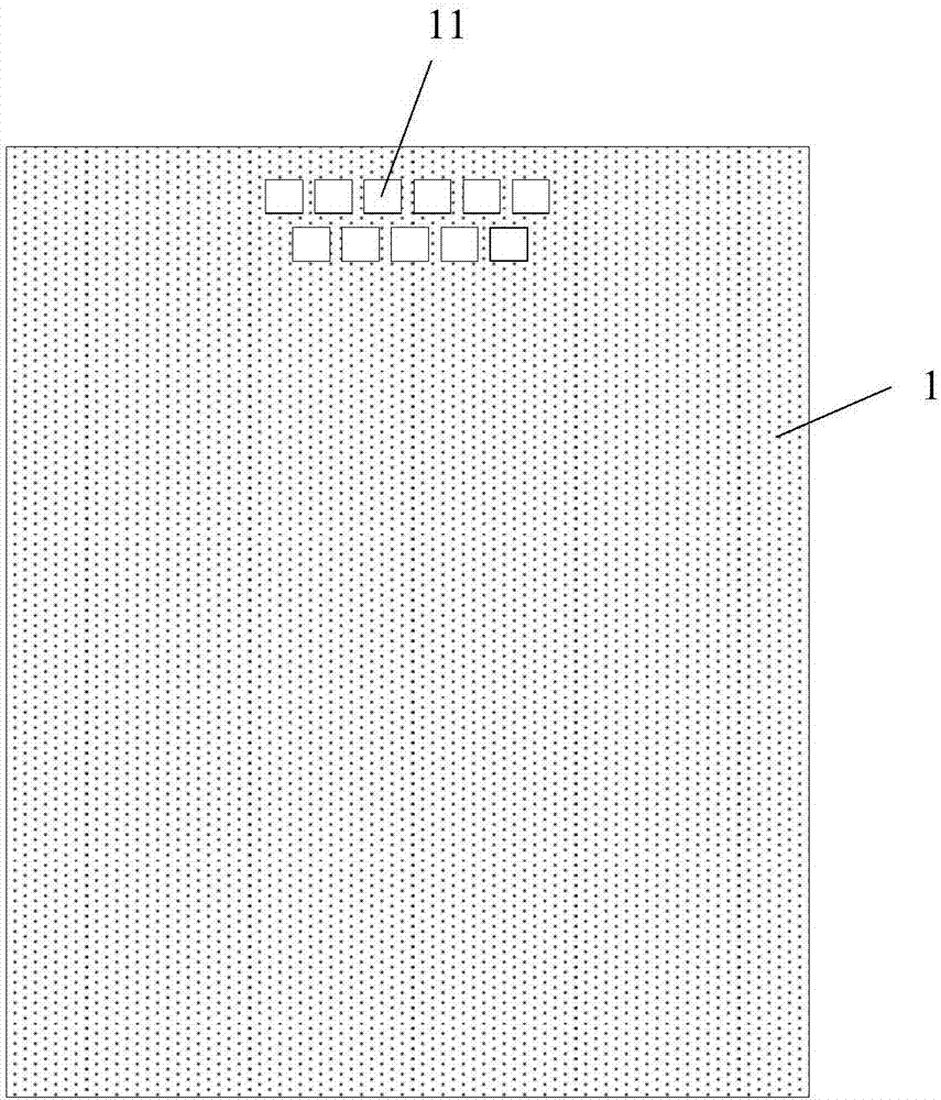
[0028] Such as figure 1 with figure 2 As shown, the display substrate includes a display structure 3, and an electronic device 5 and a base film 1 disposed on both sides of the display structure 3, wherein the display structure 3 and the base film 1 are connected by an adhesive 2, and the base film 1 is placed on the A dredging hole 11 is ...

Embodiment 2

[0058] This embodiment provides a display device, which includes the display substrate of Embodiment 1.

[0059] The display device can be: desktop computer, tablet computer, notebook computer, mobile phone, PDA, GPS, vehicle display, projection display, video camera, digital camera, electronic watch, calculator, electronic instrument, instrument, LCD panel, electronic paper, TV Computers, monitors, digital photo frames, navigators and any other products or components with display functions can be applied to multiple fields such as public display and virtual display.


PUM


Abstract

The invention belongs to the technical field of display, and particularly relates to a display substrate, a preparing method of the display substrate and a display device. The display substrate comprises a display structure, electronic devices arranged on the two sides of the display structure and a basement film, wherein the display structure is connected with the basement film through a binding agent, and dredging holes are formed in the areas, corresponding to the electronic devices, of the basement film and used for dredging deformation of the binding agent. In the display substrate, a basement film in a back film is imaged relative to an IC bonding area, through holes are formed in the basement film of the IC bonding area, so that when hot-pressing bonding is carried out, pressure-sensitive adhesive in the back film can be deformed and overflowed from the dredging holes, it is avoided that as the pressure-sensitive adhesive flows and is sunk and warped to lateral corresponding places without bumps, a display screen is sunk and warped, ACF particle packing of a display-screen warping area and lateral contact of the adjacent IC bumps are avoided, and the IC short-circuit phenomenon and the circuit breaking phenomenon caused when the display screen is sunk and deformed are avoided.

Description

technical field [0001] The invention belongs to the field of display technology, and in particular relates to a display substrate, a preparation method of the display substrate and a display device. Background technique [0002] Currently, liquid crystal display (LCD for short) and organic electroluminescent display (OLED) have become mainstream flat panel display devices, and flexible display devices are widely used in curved surfaces due to their ability to bend. The field of display, such as smart card, electronic paper, and smart label applications, covers almost all applications that traditional display devices can apply, and has gradually become a new favorite in the field of display technology. [0003] In a flexible display device, bonding an integrated circuit (IC chip) or a flexible circuit board (FPC) to a flexible substrate through an anisotropic conductive film (ACF) is a process in the preparation of a flexible display structure. One of the important processes...

Claims


Application Information

Patent Timeline
Patent Type & Authority Applications(China)
IPC IPC(8): G09F9/30
CPCG09F9/301
Inventor 谢春燕张嵩陈立强
Owner BOE TECH GRP CO LTD
Why Eureka
Try Eureka