Technological method for removing basic membrane of photoresist

A process method and technology of photoresist, applied in the direction of electrical components, semiconductor/solid-state device manufacturing, circuits, etc., can solve the problem of unclean removal

Active Publication Date: 2017-12-12
CHENGDU HIWAFER SEMICON CO LTD
View PDF8 Cites 1 Cited by
  • Summary
  • Abstract
  • Description
  • Claims
  • Application Information

AI Technical Summary

Problems solved by technology

[0005] The present invention aims to solve the technical problem of unclean remova

Method used


Image

  • Technological method for removing basic membrane of photoresist

Examples


Embodiment Construction

[0025] In order to solve the technical problem of unclean removal when removing various photoresists in the GaAs / GaN HEMT process in the prior art, the present invention further provides a process method for removing the bottom film of photoresist, which can effectively Remove the photoresist base film.

[0026] In order to solve the above-mentioned technical problems, the above-mentioned technical solutions will be described in detail below in conjunction with the accompanying drawings and specific implementation methods.

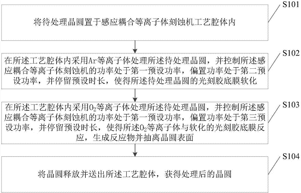
[0027] A kind of process method of removing photoresist base film provided by the invention, such as figure 1 As shown, it includes the following steps: S101, placing the wafer to be processed in the process chamber of the inductively coupled plasma etching machine, specifically including: placing the wafer to be processed on the transfer arm of the inductively coupled plasma etching machine; and then , controlling the transfer of the wafer to be processe...


PUM


Abstract

The invention relates to the field of compound semi-conductor processing manufacture and discloses a technological method for removing a basic membrane of a photoresist. The technological method comprises the following steps: sending wafers to be processed into a technological cavity of an inductive coupling plasma etcher by use of a transfer arm, and retrieving the transfer arm; after the positions of the wafers are fixed, processing the wafers to be processed in the technological cavity by Ar plasma, controlling the power of the inductive coupling plasma etcher to be first preset power and bias power to be second preset power, and staying for a preset period of time; processing the wafers to be processed in the technological cavity by O2 plasma, controlling the power of the inductive coupling plasma etcher to be first preset power and bias power to be third preset power, and staying for a preset period of time; and releasing the wafers, sending the wafers out of the technological cavity to obtain processed wafers, and further effectively removing the basic membrane of the photoresist.

Description

technical field [0001] The invention relates to the field of compound semiconductor processing and manufacturing, in particular to a process method for removing a bottom film of photoresist. Background technique [0002] Compound semiconductors represented by GaAs and GaN have shown unique performance advantages in the field of microwave radio frequency, and have increasingly become mainstream materials for high-end radio frequency chips. High electron mobility transistors (HEMT) based on GaAs and GaN materials are very suitable for high-frequency and high-power fields, and have attracted more and more attention from the industry. [0003] In the GaAs / GaN HEMT process, various photoresists are required, and in some process occasions, the photoresist is difficult to remove due to the influence of the pre-process steps, such as the photoresist mask during ion implantation after ion bombardment There will be a layer of hard-to-remove plastic shell on the edge. The photoresist ...

Claims


Application Information

Patent Timeline
IPC IPC(8): H01L21/311
CPCH01L21/31138
Inventor 孔欣
Owner CHENGDU HIWAFER SEMICON CO LTD
Why Eureka
Try Eureka