Mask layer structure, semiconductor device and manufacturing method thereof
A manufacturing method and mask layer technology, applied in semiconductor/solid-state device manufacturing, electrical components, circuits, etc., to achieve the effect of increasing the process window, improving yield and performance
- Summary
- Abstract
- Description
- Claims
- Application Information
AI Technical Summary
Problems solved by technology
Method used
Image

Examples
Embodiment 1
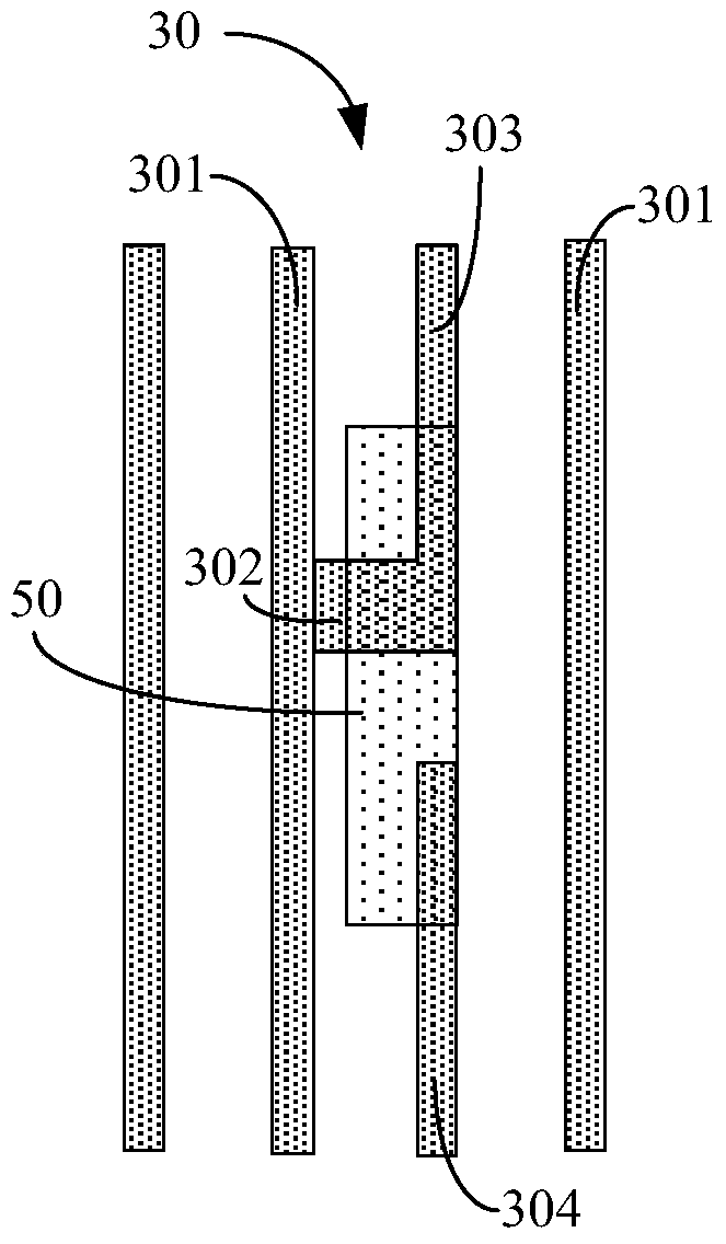
[0052] As an example, such as Figure 3A and Figure 3B As shown, the mask layer structure based on the self-aligned double pattern of the present invention includes: a substrate (not shown), and a core mask layer pattern 30 formed on the substrate.
[0053] Wherein, the substrate may include a semiconductor substrate, and the semiconductor substrate may be at least one of the materials mentioned below: silicon, silicon-on-insulator (SOI), silicon-on-insulator (SSOI), germanium-on-insulator Silicon (S-SiGeOI), silicon germanium on insulator (SiGeOI) and germanium on insulator (GeOI), etc.
[0054] Optionally, the substrate further includes a front-end device formed on the semiconductor substrate, the front-end device can be a transistor, the transistor can be used to form various circuits, and the transistor can be an ordinary transistor, a high-k metal gate transistors, fin transistors, or other suitable transistors.
[0055] The front-end device may also include various o...
Embodiment 2
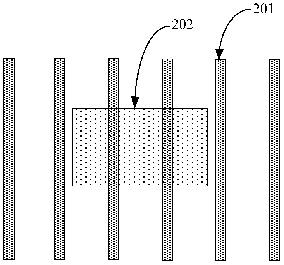
[0088] Below, refer to Figure 4A to Figure 4D A specific embodiment of the aforementioned method for manufacturing a semiconductor device will be described in detail.
[0089] The manufacturing method of the semiconductor device of the present invention is based on the SADP process, which can be used for manufacturing metal wires. In this embodiment, the manufacturing method of the present invention is mainly introduced in detail by taking the manufacturing process of metal wires as an example.
[0090] First, if Figure 4A As shown, a substrate (not shown) is provided on which a nuclear mask layer pattern 30 is formed.
[0091] Wherein, the substrate may include a semiconductor substrate, and the semiconductor substrate may be at least one of the materials mentioned below: silicon, silicon-on-insulator (SOI), silicon-on-insulator (SSOI), germanium-on-insulator Silicon (S-SiGeOI), silicon germanium on insulator (SiGeOI) and germanium on insulator (GeOI), etc.
[0092] Opti...
Embodiment 3
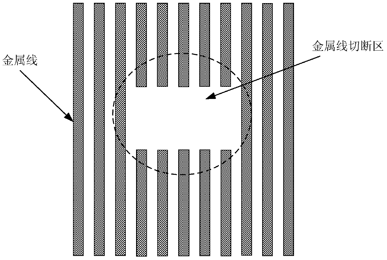
[0132] The present invention also provides a semiconductor device formed by the above-mentioned manufacturing method, the semiconductor device includes a metal wire pattern, the metal wire pattern includes a plurality of metal wires extending along the first direction, and a cut-off area is provided in the central area of the metal wire pattern. There are several metal wires extending along the first direction, and the number of the cut metal wires is an even number.
[0133] Since the semiconductor device of the present invention is manufactured by the aforementioned method, the semiconductor device of the present invention also has the same advantages on the premise that the aforementioned method has excellent technical effects.
PUM
 Abstract
Description
Claims
Application Information
 - R&D
- Intellectual Property
- Life Sciences
- Materials
- Tech Scout
- Unparalleled Data Quality
- Higher Quality Content
- 60% Fewer Hallucinations
Browse by: Latest US Patents, China's latest patents, Technical Efficacy Thesaurus, Application Domain, Technology Topic, Popular Technical Reports.
© 2025 PatSnap. All rights reserved.Legal|Privacy policy|Modern Slavery Act Transparency Statement|Sitemap|About US| Contact US: help@patsnap.com