Manufacturing method of semiconductor device, semiconductor device and electronic device
A manufacturing method and semiconductor technology, which is applied in semiconductor/solid-state device manufacturing, circuits, electrical components, etc., can solve the problems of increased sidewall roughness of key dimensions, performance that cannot meet the predetermined design, device impact, etc., and achieve good sidewall roughness High degree, good key size, good effect of device performance
- Summary
- Abstract
- Description
- Claims
- Application Information
AI Technical Summary
Problems solved by technology
Method used
Image

Examples
Embodiment 1
[0029] The following will refer to figure 2 as well as Figure 3A ~ Figure 3E A method for fabricating a semiconductor device according to an embodiment of the present invention will be described in detail.
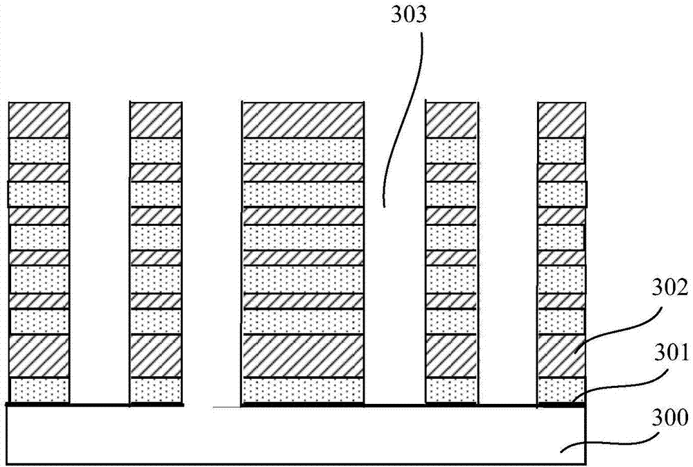
[0030] First, step 201 is performed: providing a semiconductor substrate 300, on which a stacked structure consisting of multiple layers of staggered dummy dielectric layers 301 and interlayer dielectric layers 302 is formed, the dummy dielectric The layer 301 is formed between adjacent interlayer dielectric layers 302, and a trench 303 is formed in the interlayer dielectric layer 302 and the dummy dielectric layer 301, and the trench 303 exposes the substrate 300, so formed structure such as Figure 3A shown.
[0031]Wherein, the semiconductor substrate 300 can be at least one of the materials mentioned below: Si, Ge, SiGe, SiC, SiGeC, InAs, GaAs, InP or other III / V compound semiconductors, and also includes multiple semiconductors composed of these semiconductors. ...
Embodiment 2
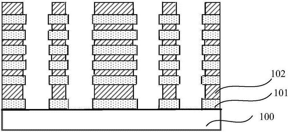
[0048] The present invention also provides a semiconductor device, such as Figure 4 As shown, the semiconductor device 400 includes: a semiconductor substrate 401, on which a multi-layer interleaved dummy dielectric layer 402 and an interlayer dielectric layer 403 are formed, and the dummy dielectric layer 402 is formed Between the adjacent interlayer dielectric layers 403, a trench 404 is formed in the interlayer dielectric layer 403 and the dummy dielectric layer 402, and a trench 404 is formed on the semiconductor substrate 401 at the bottom of the trench 404. semiconductor layer 405 .
[0049] Wherein the semiconductor substrate 401 can be at least one of the materials mentioned below: Si, Ge, SiGe, SiC, SiGeC, InAs, GaAs, InP or other III / V compound semiconductors, and also includes multilayers composed of these semiconductors The structure or the like may be silicon-on-insulator (SOI), silicon-on-insulator (SSOI), silicon-germanium-on-insulator (S-SiGeOI), silicon-germ...
Embodiment 3
[0055] Still another embodiment of the present invention provides an electronic device, including the above-mentioned semiconductor device and an electronic component connected to the semiconductor device. Wherein, the semiconductor device includes: a semiconductor substrate, on which a multi-layer interlayer dielectric layer and a dummy dielectric layer are formed, and the dummy dielectric layer is formed on an adjacent layer Between the interlayer dielectric layers, trenches are formed in the interlayer dielectric layer and the dummy dielectric layer, and a semiconductor layer is formed on the semiconductor substrate at the bottom of the trenches.
[0056]The semiconductor substrate can be at least one of the materials mentioned below: Si, Ge, SiGe, SiC, SiGeC, InAs, GaAs, InP or other III / V compound semiconductors, including multilayer structures composed of these semiconductors etc. or silicon-on-insulator (SOI), silicon-on-insulator (SSOI), silicon-germanium-on-insulator ...
PUM
 Abstract
Description
Claims
Application Information
 - R&D Engineer
- R&D Manager
- IP Professional
- Industry Leading Data Capabilities
- Powerful AI technology
- Patent DNA Extraction
Browse by: Latest US Patents, China's latest patents, Technical Efficacy Thesaurus, Application Domain, Technology Topic.
© 2024 PatSnap. All rights reserved.Legal|Privacy policy|Modern Slavery Act Transparency Statement|Sitemap