Method for electroplating copper

A technology for electroplating copper and electroplating layers, applied in circuits, electrolytic processes, electrolytic components, etc., can solve problems such as affecting the electrical conductivity of products, increasing lattice voids, affecting product yields, etc., to avoid void defects and meet filling requirements. , the effect of simple cost

Inactive Publication Date: 2017-12-22
WUHAN XINXIN SEMICON MFG CO LTD
View PDF5 Cites 1 Cited by
  • Summary
  • Abstract
  • Description
  • Claims
  • Application Information

AI Technical Summary

Problems solved by technology

[0007] In step 13, additives are added to the solution used for electroplating copper. The additives are organic substances. During the electroplating process, they may be adsorbed to the inside of copper, so that the gaps between the lattices inside the copper become larger. In the advanced copper plating process, many voids will appear in the copper plated by the electroplated wafer. When there are many small voids in the copper, after the grinding is completed, the surface will be left with pits and pits, which will affect the The performance of the product in terms of electrical conductivity will ultimately affect the yield of the product

Method used


Image

  • Method for electroplating copper
  • Method for electroplating copper
  • Method for electroplating copper

Examples


Embodiment Construction

[0040] It should be noted that, in the case of no conflict, the following technical solutions and technical features can be combined with each other.

[0041] The specific embodiment of the present invention will be further described below in conjunction with accompanying drawing:

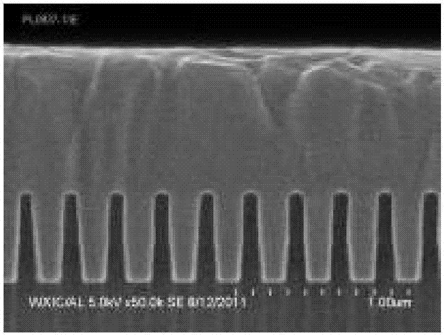
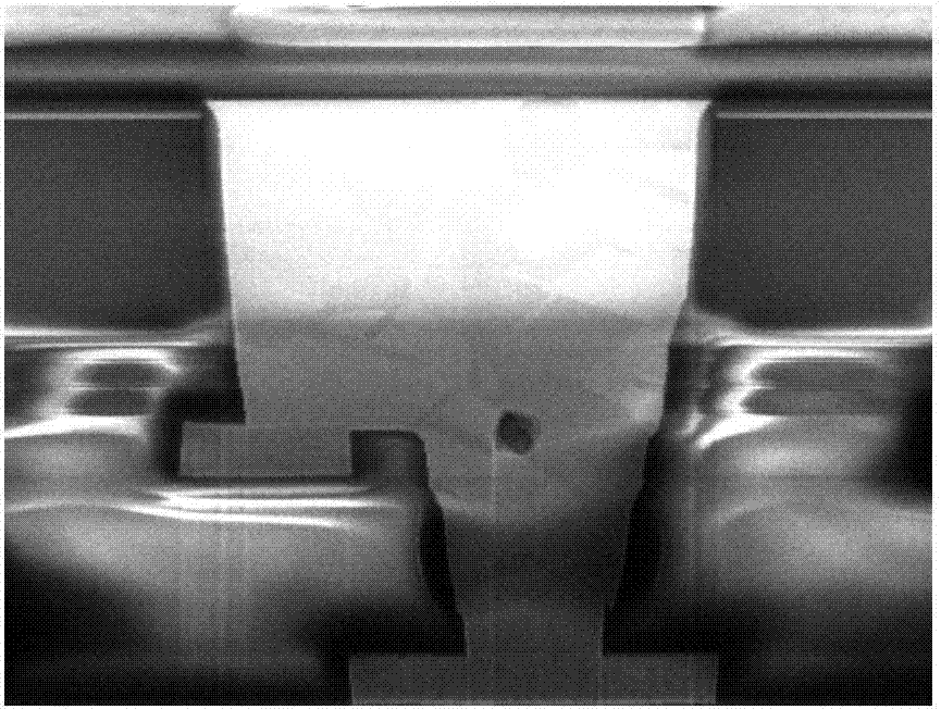
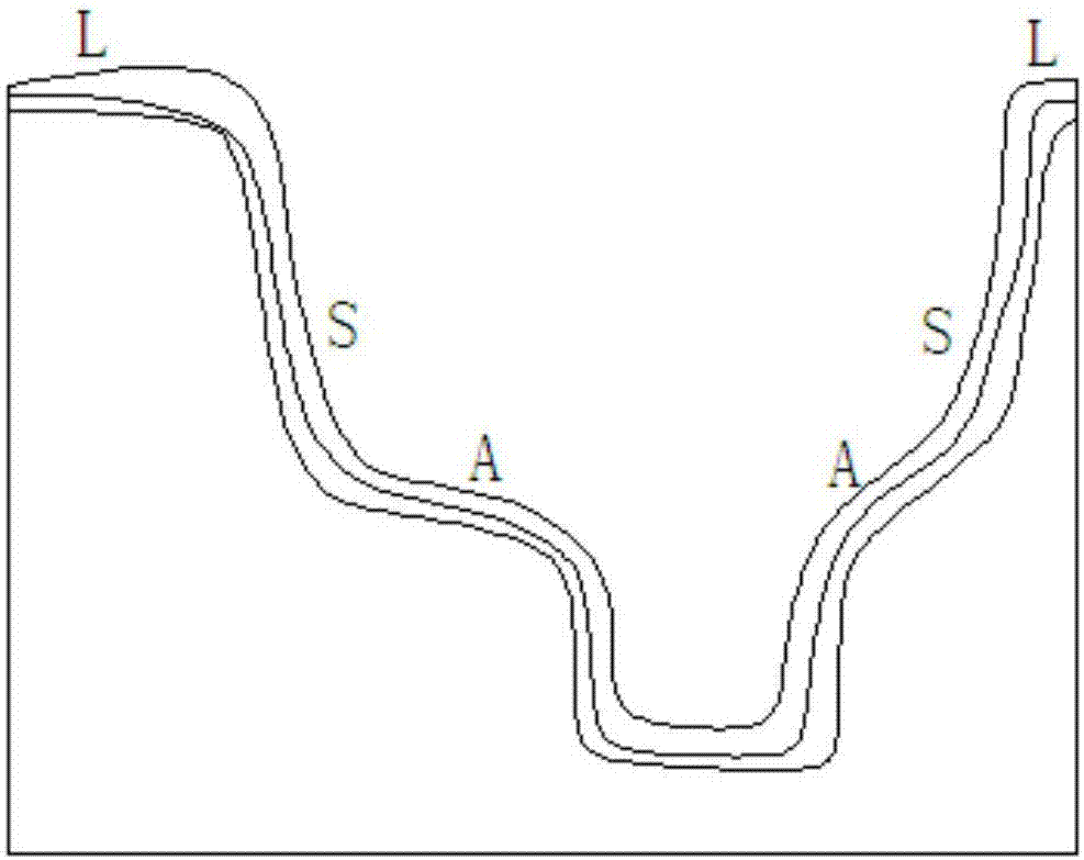
[0042] In the existing process, under the same electroplating equipment and the same additive system (L: leveler, S: inhibitor, A: accelerator), if the copper electroplating process for small-sized channels can be satisfied, then in large-sized channels trench copper plating process, such as Figure 3-5 As shown, void defects will eventually appear.

[0043] The method of electroplating copper is suitable for electroplating equipment to deposit a copper electroplating layer in the channel of the wafer. In the prior art, the above method of electroplating copper includes three stages: initial stage, second stage and overplating stage:

[0044] In the above-mentioned primary stage, the above-mentio...


PUM


Abstract

The invention provides a method for electroplating copper, and is applicable to electroplating equipment to deposit a copper electroplating layer in a channel of a wafer. The method for electroplating the copper comprises an initial stage, a second stage, a third stage, a fourth stage and the three stages of an excessive electroplating stage; and compared with the prior art, the third stage and the fourth stage are added, the rotation speed range of the wafer is increased in the initial stage while the range of electroplating current is kept unchanged, in the second stage, the third stage and the fourth stage, the rotating speed range of the wafer is kept unchanged while the range of the electroplating current is adjusted in a section-by-section mode, and the rotation speed range of the wafer and the range of the electroplating current are kept unchanged in the excessive electroplating stage. The method for electroplating the copper has the beneficial effects that technology is simple and low in cost, and finally, under the condition of the same type of the electroplating equipment and a same additive system, filling requirements of both a large-size channel and a small-size channel are met, so that a hole defect is avoided when the large-size channel is filled.

Description

technical field [0001] The invention relates to the technical field of semiconductor device manufacturing, in particular to a method for electroplating copper. Background technique [0002] In order to form copper wiring on a semiconductor wafer, it is necessary to fill vias or trenches of wiring (LSI) patterns formed on the semiconductor wafer using a copper electroplating process. [0003] The method for forming metal interconnection lines (copper wiring) in the prior art comprises the following steps: [0004] Step 11, by physical vapor deposition (PVD) method, on the bottom and sidewall of the trench, on the bottom and sidewall of the connection hole, sputter to form a barrier layer, for example, made of tantalum nitride (TaN) and tantalum (Ta) formed stacked barrier layer. The above stacked barrier layer composed of TaN and Ta is only one specific embodiment, obviously, there are many other realization methods for forming the barrier layer. [0005] Step 12, forming ...

Claims


Application Information

Patent Timeline
Patent Type & Authority Applications(China)
IPC IPC(8): C25D7/12C25D5/02C25D3/38C25D17/16C25D21/12
CPCC25D7/123C25D3/38C25D5/02C25D17/001C25D17/16C25D21/12
Inventor 龙俊舟陈红闯王鹏
Owner WUHAN XINXIN SEMICON MFG CO LTD
Why Eureka
Try Eureka