
Method for isolating shallow trench from active region

A shallow trench, active area technology, used in electrical components, semiconductor/solid-state device manufacturing, circuits, etc., can solve problems such as loss of active area area and reduction of substrate size.

Inactive Publication Date: 2017-12-22
YANGTZE MEMORY TECH CO LTD
View PDF4 Cites 0 Cited by
  • Summary
  • Abstract
  • Description
  • Claims
  • Application Information

AI Technical Summary

Problems solved by technology

[0004] However, in the prior art, after the shallow grooves of the substrate are formed, the filled thin film material will react chemically with the substrate during the annealing process, which effectively reduces the size of the substrate and causes active area loss

Method used


Image

  • Method for isolating shallow trench from active region
  • Method for isolating shallow trench from active region

Examples


Embodiment Construction

[0034] The following will clearly and completely describe the technical solutions in the embodiments of the present invention with reference to the accompanying drawings in the embodiments of the present invention. Obviously, the described embodiments are only some, not all, embodiments of the present invention. Based on the embodiments of the present invention, all other embodiments obtained by persons of ordinary skill in the art without making creative efforts belong to the protection scope of the present invention.

[0035] In order to make the above objects, features and advantages of the present invention more comprehensible, the present invention will be further described in detail below in conjunction with the accompanying drawings and specific embodiments.

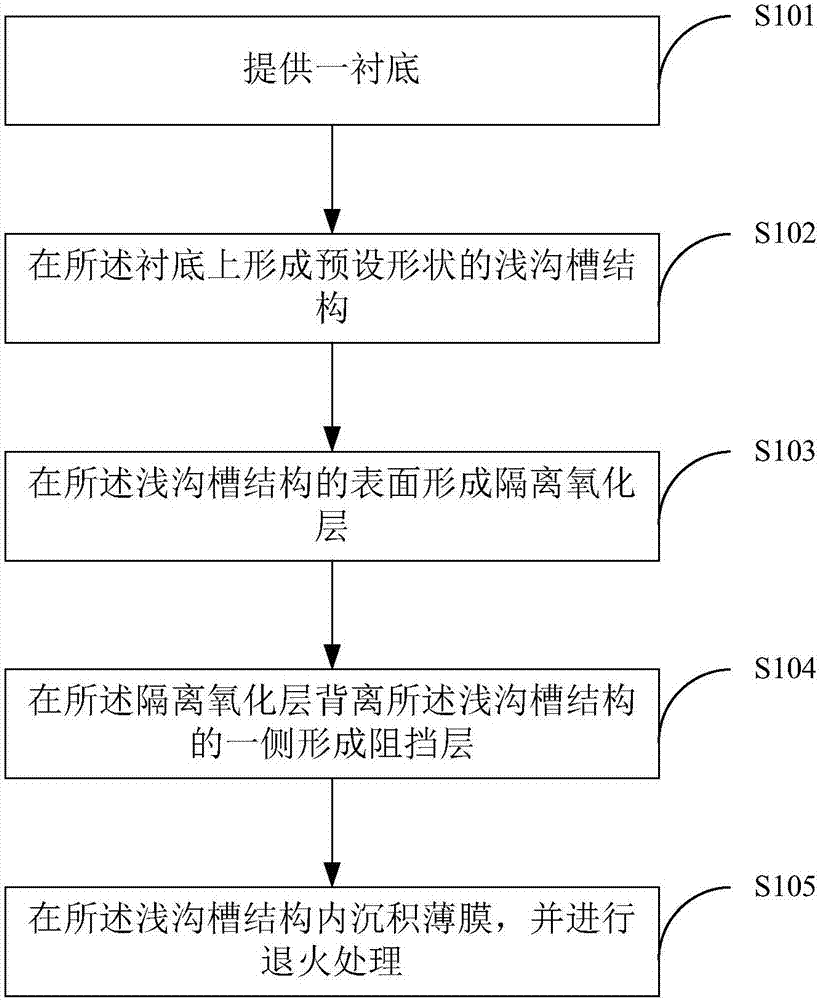
[0036] refer to figure 1 , figure 1 A method for isolating an active region by a shallow trench is provided for an embodiment of the present invention.

[0037] The methods include:

[0038] S101: Provide a sub...


PUM


Abstract

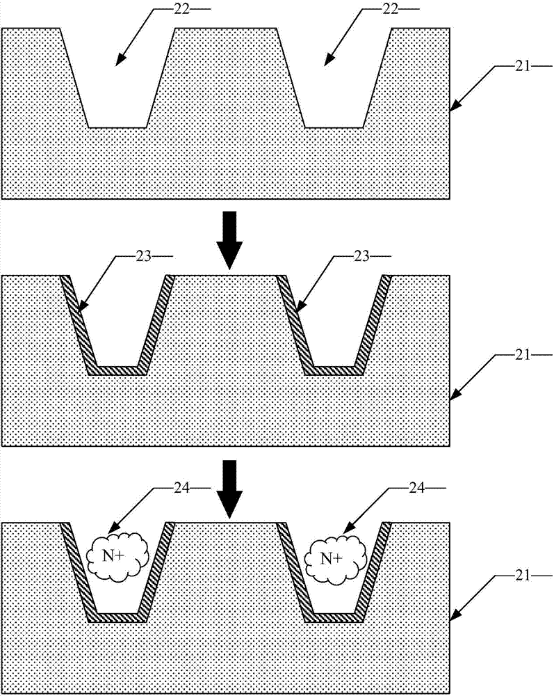
The invention discloses a method for isolating a shallow trench from an active region. The method for isolating the shallow trench from the active region comprises steps of providing a substrate, forming a shallow trench structure having a preset shape on the substrate, forming an isolation oxide layer on a surface of the shallow trench, forming a blocking layer on one side of the isolation oxide layer which is deviated from the shallow trench structure, depositing a film inside the shallow trench structure and performing annealing processing. Through arrangement of the isolation oxide layer and the blocking layer structure, the method for isolating the shallow trench from the active region removes a chemical reaction between the deposited film and the substrate during an annealing process so as to protect the size of the substrate and avoid the loss of the area of the active region.

Description

technical field [0001] The invention relates to the technical field of semiconductor technology, and more specifically, relates to a method for isolating an active region by a shallow trench. Background technique [0002] With the continuous development of science and technology, the feature size of semiconductor devices is gradually decreasing. Although the existing multi-step deposition-etching can improve the filling ability of HDP (High-Density-Plasma, high-density plasma chemical vapor deposition) , but it will make the process extremely complicated, and the deposition rate will be slow. As the number of cycles increases, the damage to the substrate caused by etching will be more serious. [0003] HARP (High-Aspect-Ratio-Process, high aspect ratio process) adopts TEOS Ramp up technology to obtain a faster growth rate under the condition of ensuring the filling capacity, making HARP gradually replace the HDP process and become the mainstream filling technology in the mar...

Claims


Application Information

Patent Timeline
Patent Type & Authority Applications(China)
IPC IPC(8): H01L21/762
CPCH01L21/76224
Inventor 余德钦周文斌张磊高永辉
Owner YANGTZE MEMORY TECH CO LTD
Learn More