Starting circuit of PWM chip of super-wide voltage auxiliary power supply

An auxiliary power supply and ultra-wide voltage technology, applied in the direction of electrical components, output power conversion devices, etc., can solve problems such as shortage of use, high cost, affecting power conversion efficiency, heat dissipation and reliability, etc., to achieve reliable work, The effect of small circuit loss

Active Publication Date: 2017-12-22
GUANGZHOU ZHONGYIGUANG ELECTRONICS TECH
View PDF16 Cites 7 Cited by
  • Summary
  • Abstract
  • Description
  • Claims
  • Application Information

AI Technical Summary

Problems solved by technology

[0003] Currently commonly used switching power supply startup circuits (such as figure 1 As shown), since the resistor R1 is always connected to the power input terminal VIN, the power consumption generated on it is P= (VIN-VCC) 2/R1. Obviously, if the switching power supply is working at a high voltage input, the power on the resistor R1 The power consumption will be very large, which will affect the power conversion efficiency, heat dissipation and reliability. At the same time, high-power resistors must be selected,

Method used


Image

  • Starting circuit of PWM chip of super-wide voltage auxiliary power supply
  • Starting circuit of PWM chip of super-wide voltage auxiliary power supply
  • Starting circuit of PWM chip of super-wide voltage auxiliary power supply

Examples


Embodiment 1

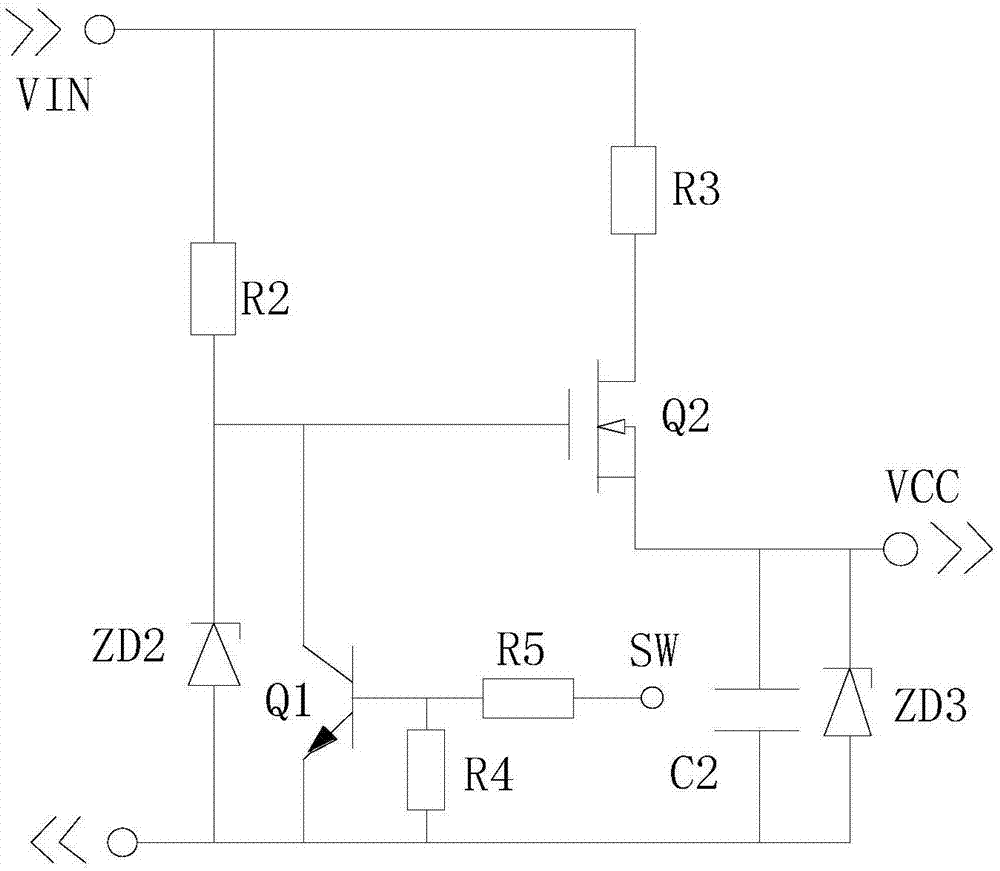
[0047] See Figure 5 , A startup circuit of an ultra-wide voltage auxiliary power supply PWM chip, including a voltage switch circuit 1, a voltage detection circuit 2 and a charging circuit 3. The voltage switch circuit 1 is composed of a MOS tube Q1, a resistor R4 and a resistor R5; a voltage detection circuit 2 is composed of MOS tube Q2, resistance R7 and resistance R8; charging circuit 3 is composed of resistance R1 and resistance R2; the drain of MOS tube Q1 is connected to one end of resistance R1 and resistance R2, and the other end of resistance R1 is connected to the voltage input interface +Vin terminal, the other end of resistor R2 is connected to the source of MOS transistor Q1 and the source of MOS transistor Q2, the gate of MOS transistor Q1 is connected to the drain of MOS transistor Q2; the gate of MOS transistor Q1 is connected to MOS transistor Q2 The connection line of the drain of the resistor R4 is also connected to the voltage input interface +Vin terminal,...

Embodiment 2

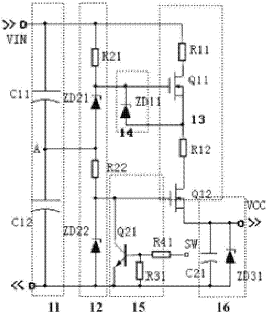
[0062] See Image 6 , Is a schematic diagram of a two-stage voltage divider series circuit, when applied to 100-1000VDC, the advantages are obvious; the explanation is as follows, when the minimum input voltage is 100VDC, the charging current is set to: 50uA, then the charging resistance value is: R1=R2 =R3=100VDC / 50uA=2MΩ, the same as the above analysis, when input voltage, the charging current is only: I=Vinmax / (R1+R2+R3)=1000VDC / 6MΩ=166mA, the current change is only 1:3. The power loss is: P=I*Vinmax=166mW. Image 6 The voltage of MOS tube Q1 and MOS tube Q3 should be: V Q1 =V Q3 =1 / 3Vinmax=330VDC.

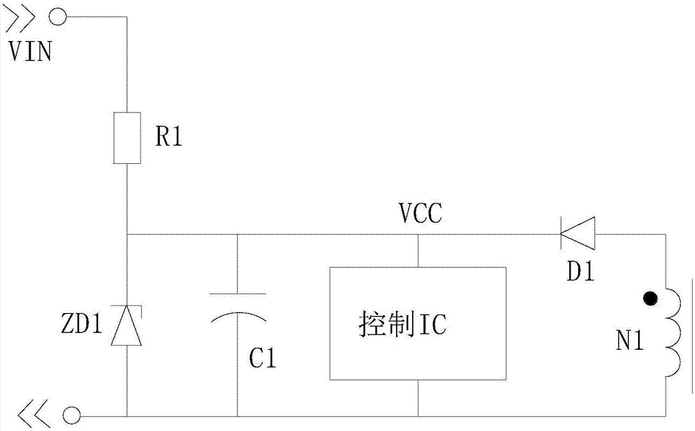
[0063] Figure 1-Figure 4 , The charging current is 50-500uA, the current change is very large, nearly 1:10, and the power loss is P=I*Vinmax=500mW.

[0064] figure 2 The voltage in the MOS tube Q2 should be V Q2 =Vinmax=1000VDC, image 3 In Q11, Q12 is V Q11 =V Q12 =1 / 2Vinmax=500VDC.

Embodiment 3

[0066] See Figure 7 , Is a schematic diagram of a three-stage voltage divider series circuit. When applied to 100-2000VDC, the advantages are more prominent; the explanation is as follows, when the minimum input voltage is 100VDC, the charging current is set to: 50uA, then the charging resistance value is: R1=R2 =R3=R41=100VDC / 50uA=2MΩ, the same as the above analysis, when input voltage, the charging current is only: I=Vinmax / (R1+R2+R3+R41)=1000VDC / 8MΩ=125uA, the current change is only 1:2.5. The power loss is: P=I*Vinmax=250mW. Figure 7 The voltage of Q1, Q3, and Q5 should be: V Q1 =V Q3 =V Q5 =1 / 4Vinmax=500VDC.

[0067] Figure 1-Figure 4 , The charging current is 50-1000uA, the current change is very large, nearly 1:20, and the power loss is P=I*Vinmax=2000mW.

[0068] figure 2 The voltage in the MOS tube Q2 is V Q2 =Vinmax=2000VDC, image 3 , Figure 4 In the MOS tube Q11, MOS tube Q12, Qa, Qb are V Q11 =V Q12 =1 / 2Vinmax=1000VDC.

[0069] Among the above points 4 and 5, in ...


PUM


Abstract

The present invention discloses a starting circuit of a PWM chip of a super-wide voltage auxiliary power supply. The circuit comprises a voltage switching switch circuit, a voltage detection circuit and a charging circuit; the voltage switching switch circuit comprises a MOS tube Q1, a resistor R4 and a resistor R5; the voltage detection circuit comprises a MOS tube Q2, a resistor R7 and a resistor R8; and the charging circuit comprises a resistor R1 and a resistor R2. The starting circuit of the PWM chip of the super-wide voltage auxiliary power supply can provide stable charging current for the PWM chip VCC no matter how the input voltage is changed, the relative change amount is small; and when the power supply generates faults, the chip can restarted and cannot enter a locking state, after the faults are eliminated, the chip can be restarted with no need for power-off restarting, especially the circuit works in the ultrahigh voltage, the circuit loss is less than the loss of a routine circuit.

Description

Technical field [0001] The invention relates to a power supply module and a switching power supply PWM auxiliary power starting circuit, in particular to a starting circuit of an ultra-wide voltage auxiliary power supply PWM chip; the input voltage can be as wide as 100-2000V. Background technique [0002] In photovoltaic inverters and ultra-high voltage DC transmission systems, the voltage range is very wide, as low as one hundred volts and as high as more than four thousand volts. Therefore, it is difficult to design the auxiliary power supply of the system, especially the design of the high-voltage shoulder circuit. Difficulty. On the one hand, it is necessary to find electronic components that can withstand high voltages. On the other hand, from the perspective of reliability, it is necessary to reduce the circuit loss of the shoulder moving part to prevent heat damage to key components. [0003] Currently commonly used switching power supply startup circuits (such as figure 1...

Claims


Application Information

Patent Timeline
IPC IPC(8): H02M1/36
CPCH02M1/36
Inventor 王中于王生辉
Owner GUANGZHOU ZHONGYIGUANG ELECTRONICS TECH
Why Eureka
Try Eureka