Device and method for increasing circuit board wiring density

A line density and circuit board technology is applied in the field of devices for increasing the wiring density of the circuit board, which can solve the problems of reducing the wiring density of the circuit board, etc., and achieve the effects of improving the timing accuracy, speeding up the etching speed, and improving the degree of refinement.

Active Publication Date: 2019-07-09
CHANGSHU MUTUAL TEK CO LTD
View PDF5 Cites 0 Cited by
  • Summary
  • Abstract
  • Description
  • Claims
  • Application Information

AI Technical Summary

Problems solved by technology

[0008] Still another object of the present invention is to provide a device and method for increasing the wiring density of a circuit board, which uses a protective sleeve to reduce the degree of invasion of the side wall of the conductive circuit by the etching solution, and solves the problem of reducing the wiring density of the circuit board due to serious side erosion. technical problem

Method used


Image

  • Device and method for increasing circuit board wiring density
  • Device and method for increasing circuit board wiring density
  • Device and method for increasing circuit board wiring density

Examples


Embodiment 1

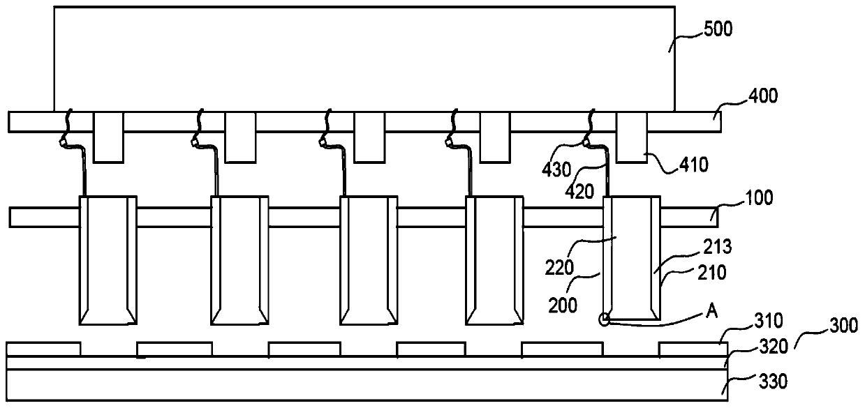
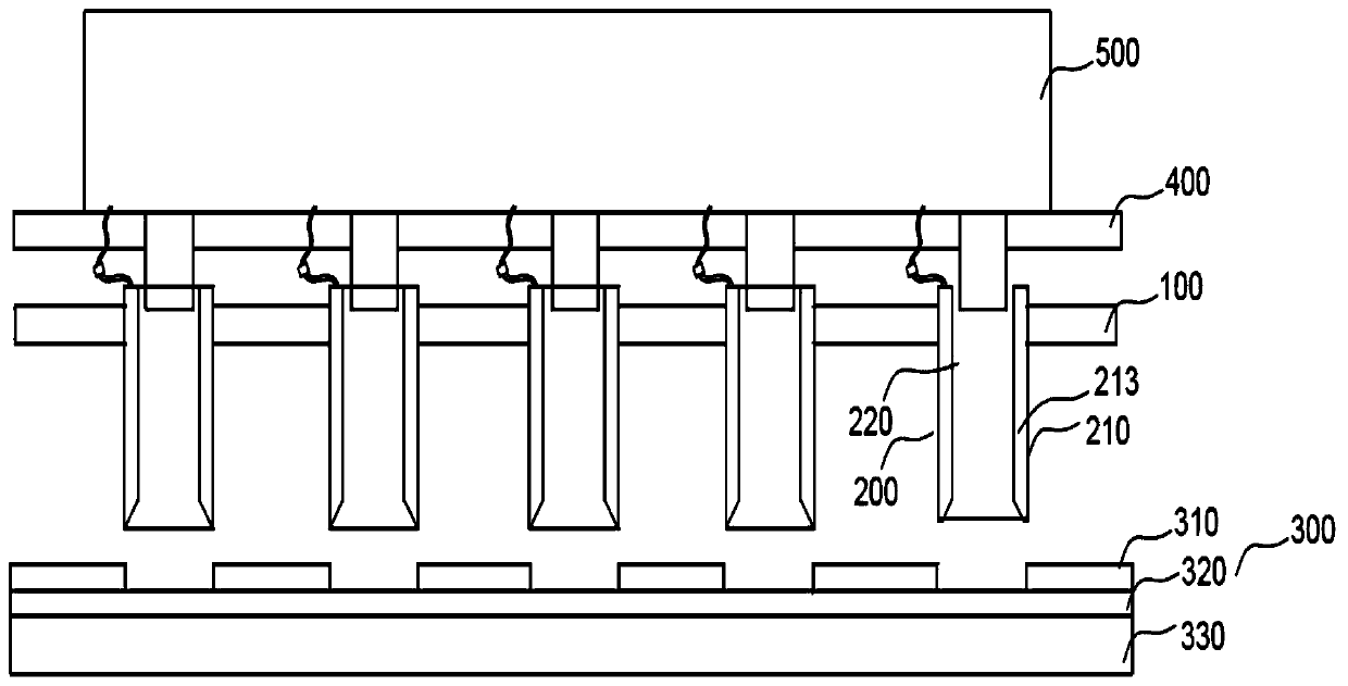
[0042] The invention provides a device and a method for increasing the wiring density of a circuit board, such as Figure 1-5 As shown, it includes a mask plate, a pressing plate 100, a protective sleeve 200 and a moving plate 400, wherein the mask plate is movably arranged on the upper end of the circuit board 300 to be etched, and is used for masking the photoresist on the circuit board 300 , the mask plate is provided with a number of through holes, after masking, exposure, and development, the photoresist 310 in the corresponding area of ​​the through holes is removed to expose the conductor part to be etched, and then the exposed conductor is etched , the remaining conductor is the conductive line.

[0043] The pressing plate 100 is movably arranged on the upper end of the mask, and after the mask is completed, the mask can be removed, and the mask can be kept in place.

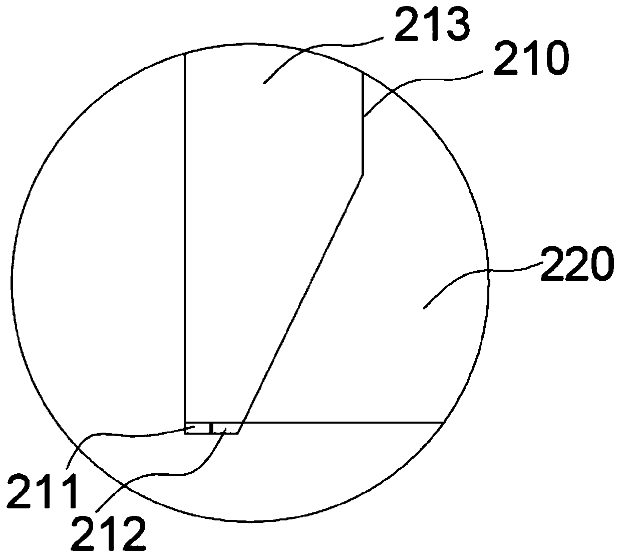
[0044] The protective sleeve 200 is a cylindrical structure whose cross-section is consistent with t...


PUM


Abstract

The invention discloses a device and method for increasing the wiring density of a circuit board. The device comprises a mask plate, a pressure plate, a protection sleeve and a moving plate. The upper end of the protection sleeve penetrates through the bottom of the pressure plate. The protection sleeve is formed by splicing a plurality of side plates. The side plates are provided therein with a hollow chamber. A nozzle is embedded in the bottom of the hollow chamber, emits solutions obliquely downward, and communicates with the hollow chamber. The shapes and the positions of the protection sleeves correspond to those of through holes on the mask plate one to one. The upper end of moving plate is provided with a closed container containing an etching solution. A plurality of first pipes and second pipes penetrate through the moving plate. The upper end of each first pipe communicates with the closed container. The lower end of each first pipe is aligned with the upper port of the corresponding protection sleeve. The upper end of the hollow chamber communicates with the second pipe via a delivery pump. The device and method solve a decrease in the wiring density of the circuit board due to serious undercut.

Description

technical field [0001] The invention relates to the technical field of circuit board preparation, and more specifically, the invention relates to a device and a method for increasing wiring density of a circuit board. Background technique [0002] Today is the era of communication, fast, light, multi-tasking and high quality are the most basic functions of related electronic or optoelectronic products, so the design and manufacture of related products must be oriented towards light, thin, multi-functional, fast, and low price direction of development. [0003] Based on this, High Density Interconnect (HDI) substrates with thin lines and tiny holes as a function of carrying assembly functions will emerge as the times require, and the demand for circuit miniaturization technology will become increasingly urgent, and the quality control requirements will also increase. It is becoming more and more stringent, which means that when the line width and line spacing become finer, t...

Claims


Application Information

Patent Timeline
Patent Type & Authority Patents(China)
IPC IPC(8): H05K3/06
CPCH05K3/068H05K2203/074
Inventor 陈依平褚鸿霖
Owner CHANGSHU MUTUAL TEK CO LTD
Why Eureka
Try Eureka