Driving circuit, switching control circuit, and switching device

A technology of switching control circuit and driving circuit, which is applied in the field of driving circuit, switching control circuit and switching device, can solve the problems of low FET201 and cannot be turned on at high speed, etc., and achieve the effect of stabilizing the driving current

Active Publication Date: 2018-01-02
新唐科技日本株式会社
View PDF4 Cites 5 Cited by
  • Summary
  • Abstract
  • Description
  • Claims
  • Application Information

AI Technical Summary

Problems solved by technology

[0004] In the above structure, the threshold value of the normally-off junction FET 201 is as low as 2.

Method used


Image

  • Driving circuit, switching control circuit, and switching device
  • Driving circuit, switching control circuit, and switching device
  • Driving circuit, switching control circuit, and switching device

Examples


Embodiment 1

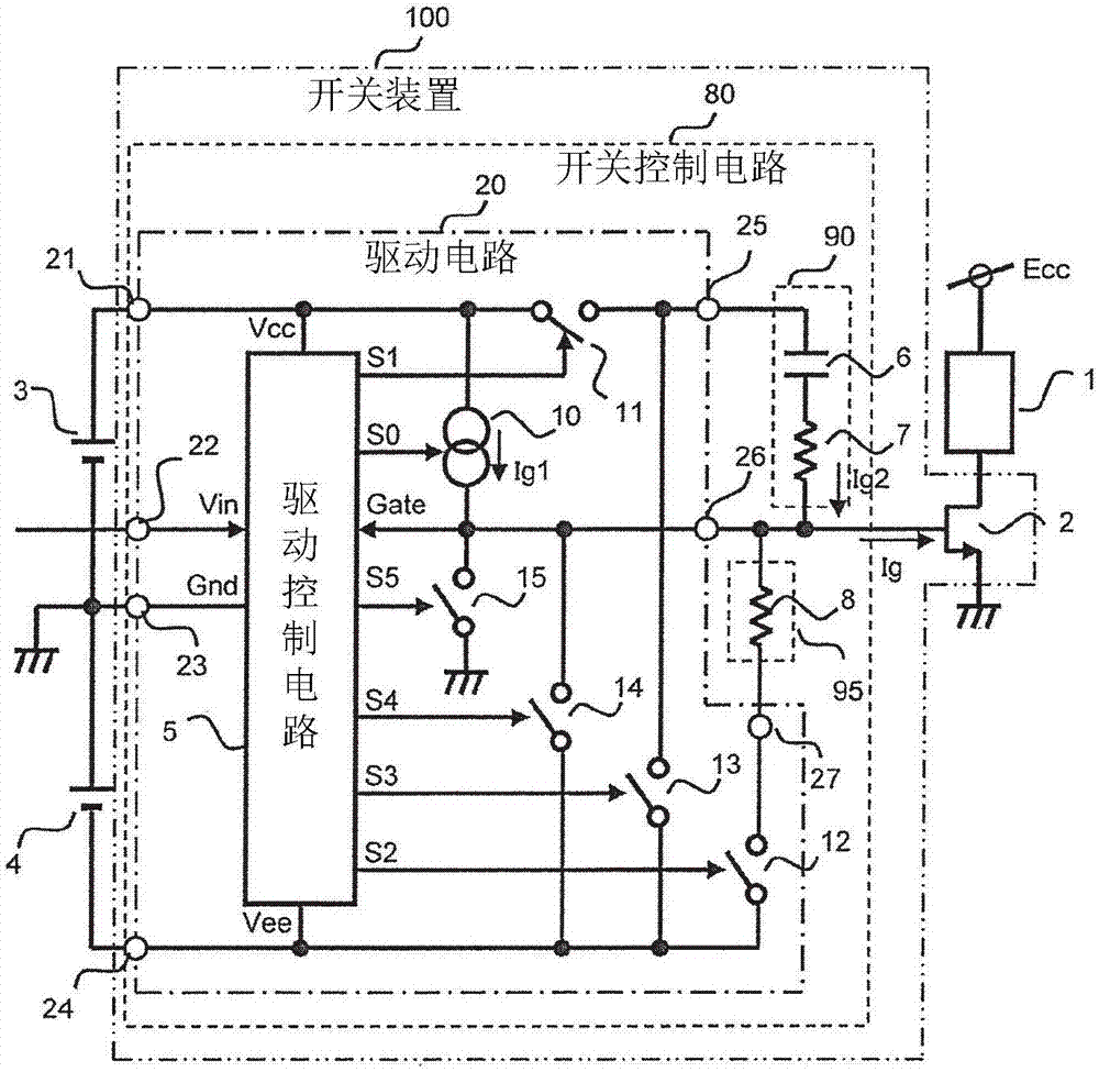
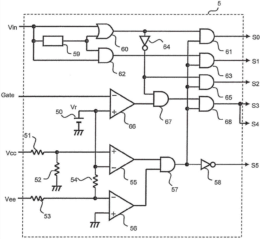
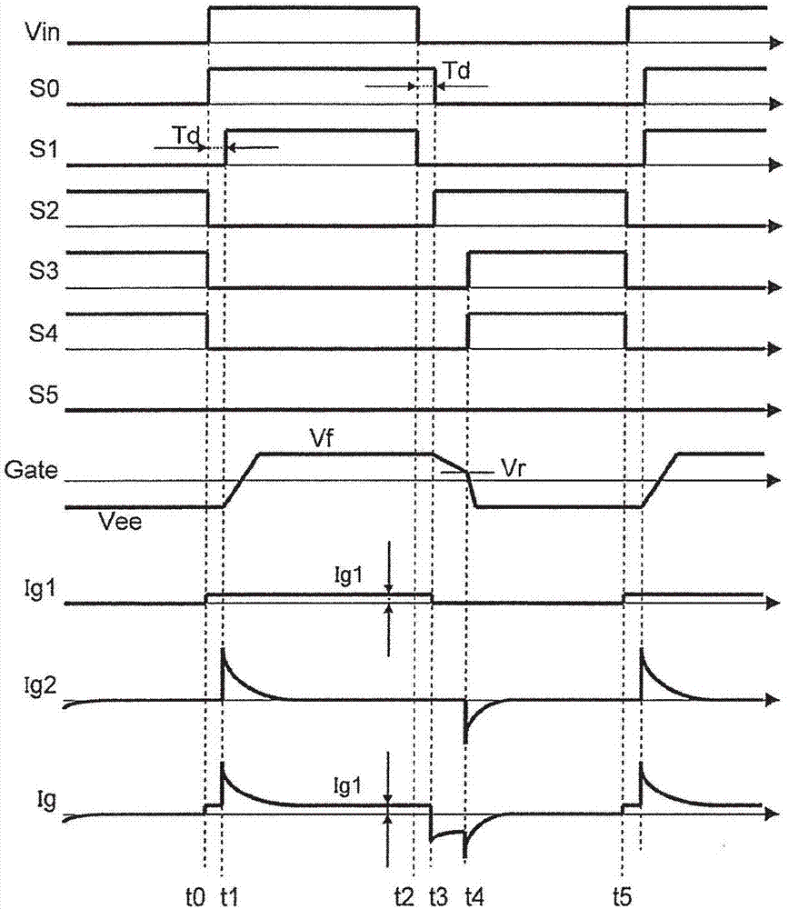
[0038] figure 1 It is a diagram showing the circuit configuration of the switching device 100 and the load 1 according to the first embodiment, figure 2 is a diagram showing an example of the circuit configuration of the drive control circuit 5, image 3 It is a diagram showing signal waveforms of the switching device 100 according to the first embodiment.

[0039] [1-1. Structure of switchgear]

[0040] exist figure 1 Among them, the switching device 100 includes a switching element 2 and a switching control circuit 80 . The switching element 2 has a first terminal as a drain terminal, a second terminal as a source terminal, and a control terminal as a gate terminal. The switching element 2 is a voltage application-current driving type switching element, for example, GaN-GIT. The pulse-like power supply voltage Ecc is applied to the load 1 by the on-off operation of the switching element 2 .

[0041] Furthermore, the current Ig is a current flowing into the gate term...

Embodiment 2

[0083] Figure 5 It is a circuit diagram illustrating a self-opening phenomenon of a conventional switch device described in Patent Document 2 (International Publication No. 2010 / 070899). The figure shows that in a general bridge structure, the high-side switch 320 and the low-side switch 301 are connected in a vertical arrangement. According to this configuration, when the high-side switch 320 is turned on, charging current flows to the parasitic capacitance 307 between the drain and the gate of the low-side switch 301, and the gate voltage of the low-side switch 301 may rise. , to become self-opening. Like this conventional switching device, the gate-source voltage threshold voltage for turning on is low, or the drain-gate parasitic capacitance is large and the gate-source input capacitance is small. In the case of high-speed switching elements, there is a problem that self-turn-on tends to occur.

[0084] On the other hand, according to the switch device 110 according to...

Embodiment 3

[0114] In Embodiment 1, the rapid charging of the gate terminal is carried out only by the drive path via the first impedance circuit which is a CR series circuit. However, the switch control circuit according to this embodiment is not limited to such a method. If the absolute value of the negative power supply potential Vee is large and the gate capacitance of the switching element 2 is large, the charging current from the drive path via the first impedance circuit is large at the beginning of supply, but as the gate capacitance and the drive capacitor The charge decreases exponentially. Therefore, when the gate voltage reaches the turn-on threshold voltage of the switching element 2, the charging current decreases, and high-speed turn-on may not be possible. In this embodiment, the problem can be solved by using another gate driving path in addition to the first impedance circuit.

[0115] Hereinafter, the drive circuit, switch control circuit, and switch device according t...


PUM


Abstract

A driving circuit (20) for driving a switching element in response to an input signal Vin, wherein the driving circuit (20) is provided with a positive power supply terminal (21) fed with a positive voltage Vcc, an input terminal (22) into which an input signal Vin is inputted, a ground terminal (23) connected to the source of the switching element (2), a first output terminal (25) capable of outputting a positive voltage Vcc in response to an input signal Vin, a current source circuit (10), and a second output terminal (26) connected to the current source circuit (10). The driving circuit (20) feeds a current Ig2, in which the positive voltage Vcc outputted from the first output terminal (25) is converted by a first impedance circuit (90), and a current Ig1 outputted from the current source circuit (10) through a second output terminal (26), to a gate, and thereby drives the switching element (2).

Description

technical field [0001] The present invention relates to a drive circuit, a switch control circuit and a switch device. Background technique [0002] Patent Document 1 discloses a semiconductor circuit using a normally-off junction FET as a switching element. [0003] Figure 12 It is a circuit diagram of the semiconductor circuit described in patent document 1. The semiconductor circuit shown in this figure consists of a normally closed junction FET (switching element) 201, a gate switch module 203, a diode 213, a Zener diode 214, a freewheeling diode 202, a feedback capacitor 207, an input capacitor 208, and parasitic Diode 209 constitutes. Junction FET 201 is disposed between drain terminal 204 and source terminal 205 . The gate switch module 203 is disposed between the gate terminal 206 and the source terminal 205 of the junction FET 201, and has a gate resistor 211, a gate power supply 212 for applying a voltage to the junction FET 201, and a gate resistor 212. 211 i...

Claims


Application Information

Patent Timeline
IPC IPC(8): H02M1/08H03K17/04H03K17/687
CPCH02M1/08H02M3/073H02M3/158H03K17/04123H03K17/163
Inventor 石井卓也川上佳人上原孝太片濑银河
Owner 新唐科技日本株式会社
Why Eureka
Try Eureka