Encapsulation structure of silicon-based biosensor chip

A sensor chip and packaging structure technology, applied in the direction of analysis materials, instruments, etc., can solve problems such as chip packaging difficulties, and achieve the effects of improved test sensitivity, small size, and stable working temperature

Active Publication Date: 2018-01-05
CHINA ELECTRONIC TECH GRP CORP NO 38 RES INST
View PDF6 Cites 5 Cited by
  • Summary
  • Abstract
  • Description
  • Claims
  • Application Information

AI Technical Summary

Problems solved by technology

Through this packaging scheme, the constant temperature and high-efficiency detection of silicon-based biosensing chips can be realized, which solves the problem of difficult chip packaging

Method used


Image

  • Encapsulation structure of silicon-based biosensor chip
  • Encapsulation structure of silicon-based biosensor chip
  • Encapsulation structure of silicon-based biosensor chip

Examples


Embodiment Construction

[0024] The present invention will be described in detail below in conjunction with the accompanying drawings.

[0025] In the description of the present invention, it should be noted that the orientation or positional relationship indicated by the terms "upper", "lower", etc. is based on the orientation or positional relationship shown in the drawings, and is only for the convenience of describing the present invention and simplifying the description. It is not intended to indicate or imply that the referred device or element must have a particular orientation, be constructed in a particular orientation, and operate in a particular orientation, and thus should not be construed as limiting the invention. In addition, the terms "first", "second", and "third" are used for descriptive purposes only, and should not be construed as indicating or implying relative importance.

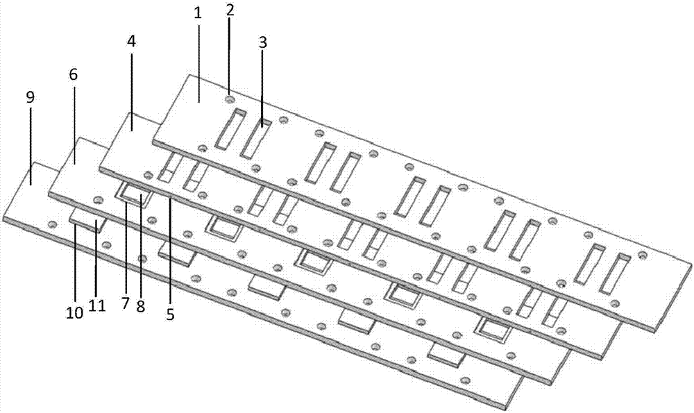
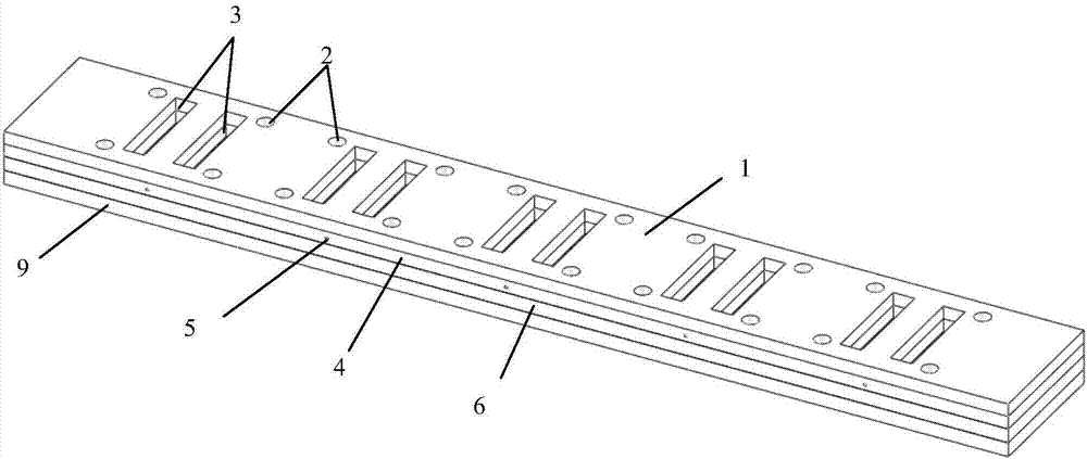
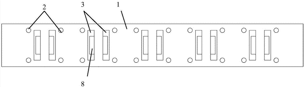
[0026] Such as Figure 1-8 As shown, a packaging structure of a silicon-based biosensor chip includes a fi...


PUM


Abstract

The invention relates to encapsulation of a microelectronic biosensor chip, in particular to an encapsulation structure of a compact multi-channel temperature-controllable silicon-based biosensor chip. The structure includes a first board, a second board and a third board, wherein the first board, the second board and the third board are sequentially overlapped in seamless joint mode; the second board is provided with a straight slot penetrating through the surface of the second board, the silicon-based biosensor chip is placed in the straight slot, a gap is formed between the bottom surface of the silicon-based biosensor chip and the surface of the third board, and the gap is filled with heat-conduction glue; the portion, directly facing the silicon-based biosensor chip, of the surface ofone side, attached to the second board, of the first board is provided with a micro flow groove, and the micro flow groove and the top surface of the silicon-based biosensor chip form a chamber usedfor containing to-be-detected liquid. According to the encapsulation structure of the silicon-based biosensor chip, the whole structure is compact, the size is small and the integration degree is high. The design of a laterally introduced PDMS micro flow channel makes the to-be-detected liquid fully contact with a microring resonator structure on the surface of a silicon wafer, and the testing sensitivity is greatly improved.

Description

technical field [0001] The invention relates to the packaging of a microelectronic biosensing chip, in particular to a packaging structure of a compact temperature-controllable multi-channel silicon-based biosensing chip. Background technique [0002] Silicon material is a traditional microelectronic material, which has been widely used in the field of CMOS. In recent years, silicon photonics has gradually become popular, and great breakthroughs have been made in photoelectric modulators, splitters, and various active and passive devices. At the same time, researchers have gradually applied silicon photonics to various sensing fields, especially direction of biosensing. When the microring resonator is processed on a silicon chip, when the concentration of the substance to be measured changes, the effective refractive index of the microring waveguide will change, which will cause the resonant peak of the microring to drift. The amount of drift is measured by an external spec...

Claims


Application Information

Patent Timeline
Patent Type & Authority Applications(China)
IPC IPC(8): G01N35/00
Inventor 丁立金里方悄然赵恒孟秋实周杰郭进
Owner CHINA ELECTRONIC TECH GRP CORP NO 38 RES INST
Why Eureka
Try Eureka