
Transistor packaging structure

A packaging structure and transistor technology, applied in the direction of electric solid-state devices, semiconductor devices, semiconductor/solid-state device components, etc., can solve problems such as voltage isolation, reduce material requirements, improve system stability and reliability, and simplify the installation process Effect

Inactive Publication Date: 2018-01-05
SHANGHAI JINGLIANG ELECTRONICS TECH
View PDF7 Cites 0 Cited by
  • Summary
  • Abstract
  • Description
  • Claims
  • Application Information

AI Technical Summary

Problems solved by technology

[0003] In view of the defects in the prior art, the purpose of the present invention is to provide a transistor packaging structure that not only retains the high power dissipation of TO-220 packaging, but also solves the problem of voltage isolation between device positioning holes and heat sinks

Method used


Image

  • Transistor packaging structure
  • Transistor packaging structure
  • Transistor packaging structure

Examples


Embodiment Construction

[0020] The present invention will be described in detail below in conjunction with specific embodiments. The following examples will help those skilled in the art to further understand the present invention, but do not limit the present invention in any form. It should be noted that those skilled in the art can make several changes and improvements without departing from the concept of the present invention. These all belong to the protection scope of the present invention.

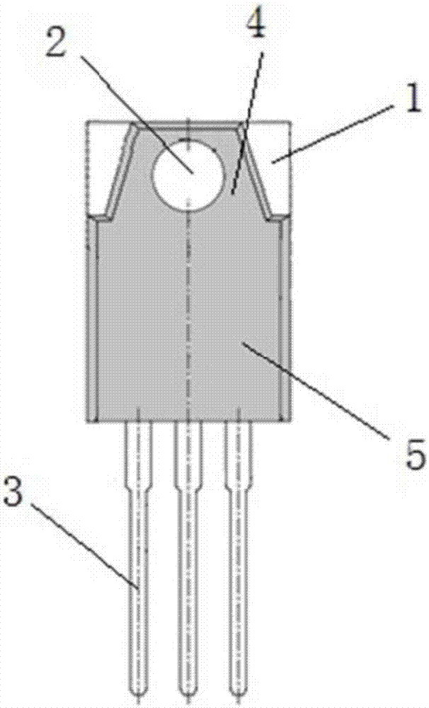
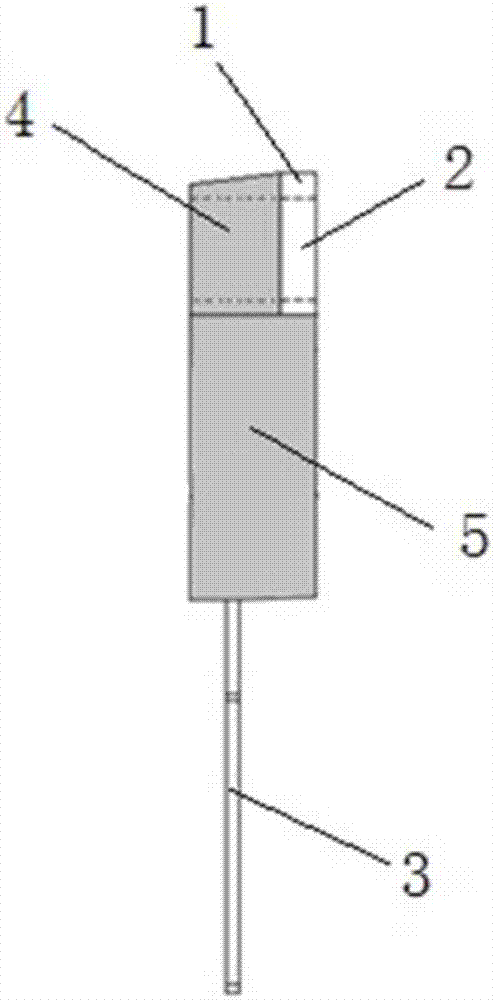
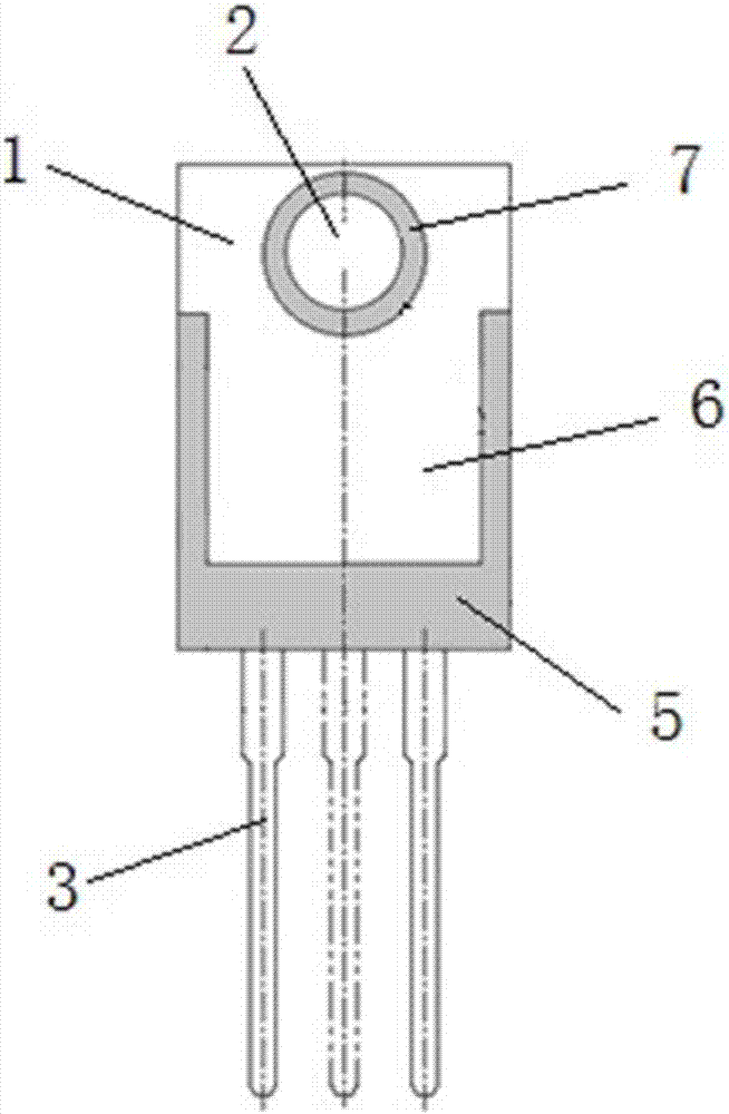
[0021] Such as Figure 1 ~ Figure 3 As shown, the transistor package structure of the present invention can be seen from the front and side of the package, the positioning hole 2 of the metal base 1 on the upper part of the device is partially covered by the first packaging unit 4 and the second packaging unit 5 made of plastic encapsulant, and the pins 3 from The bottom of the second packaging unit 5 emerges. It can be seen from the back of the package that the positioning hole 2 of the metal base 1 i...


PUM


Abstract

The invention provides a transistor packaging structure. The transistor packaging structure comprises a pedestal, pins and a packaging body; a positioning hole is formed in the pedestal; one terminalof the pin is connected to the bottom of the pedestal; the packaging body is arranged on the pedestal; the packaging body comprises a first packaging unit and a second packaging unit; the first packaging unit is arranged on the upper part of one side of the pedestal; a through hole is formed in the first packaging unit; the shape and the position of the through hole are matched with that of a positioning hole; the second packaging unit is arranged on the lower part of one side of the pedestal; and the second packaging unit is connected to the first packaging unit. Compared with the prior art,the transistor packaging structure can isolate voltage without installing an insulator. A large area of metal exposure on a packaged bottom can effectively transmit out heat inside a device and can satisfy the need for big power application. The transistor packaging structure can reduce material requirements of a terminal application manufacture, simplifies an installation process, reduces an artificial cost and eventually improves system stability and reliability.

Description

technical field [0001] The invention belongs to the field of semiconductors, and in particular relates to an improvement of a transistor outer packaging structure. Background technique [0002] TO-220 transistor outline package (Transistor Outline Package) is a package widely used in power devices. It is characterized by a large area of ​​metal on the back of the component, which can be connected to a heat sink for heat dissipation. Therefore, TO-220 can provide higher of dissipated power. Generally, the metal on the back of the TO-220 packaged device is connected to the system bus bar, and there is a relatively high voltage. When using metal nuts to fix the TO-220 device to the heat sink, it is necessary to add an insulator between the metal positioning hole and the nut to isolate the voltage. Therefore, an operation step of installing insulators is added when installing TO-220 packaged power devices, which increases the material cost and labor cost of terminal applicatio...

Claims


Application Information

Patent Timeline
IPC IPC(8): H01L23/31H01L23/367
CPCH01L2924/181H01L2924/00012
Inventor 廖奇泊徐维周雯
Owner SHANGHAI JINGLIANG ELECTRONICS TECH
Features
  • Generate Ideas
  • Intellectual Property
  • Life Sciences
  • Materials
  • Tech Scout
  • Unparalleled Data Quality
  • Higher Quality Content
  • 60% Fewer Hallucinations
Learn More