Mask for encapsulation of organic light emitting diode (OLED) thin film

A thin-film packaging and masking technology, applied in the field of masking, can solve the problems of tearing and cracking, a large number of particles, affecting the effect of thin-film packaging, etc., and achieve the effect of guaranteeing the effect.

Inactive Publication Date: 2018-01-05
WUHAN CHINA STAR OPTOELECTRONICS SEMICON DISPLAY TECH CO LTD
View PDF5 Cites 5 Cited by
  • Summary
  • Abstract
  • Description
  • Claims
  • Application Information

AI Technical Summary

Problems solved by technology

[0004] like Figure 3a As shown, in the process of using the mask plate, in order to avoid the shadow effect (shadow effect), the mask plate 302 needs to be closely attached to the substrate 301 during film formation, the mask plate 302 forms an opening 304, and the thin film packaging material A continuous thin film 303 will be generated at the substrate 301, the mask plate 302 and the junction of the two; after film formation is completed, as Figure 3b As shown, the mask plate 310 needs to rise to facilitate the pick-and-place action of the substrate 311. At this time, the continuous film 312 will be at the junction of the substrate 311 and the mask plate 310 due to the rise of the mask plate 310. 313 in area A is broken, resulting in a large number of particles, and particles are an important factor for the success or failure of thin-film packaging. When there are many particles, thin-film packaging is often prone to failure
[0005] To sum up, in the thin film encapsulation process of the conventional OLED thin-film encapsulation mask, a continuous thin film of the substrate, the mask, and the junction of the two will be formed. After the film formation is completed, when the mask is raised, the continuous The thin film will be torn and broken due to the rise of the mask plate, resulting in a large number of particles, which will affect the effect of thin film encapsulation

Method used


Image

  • Mask for encapsulation of organic light emitting diode (OLED) thin film
  • Mask for encapsulation of organic light emitting diode (OLED) thin film
  • Mask for encapsulation of organic light emitting diode (OLED) thin film

Examples


Embodiment Construction

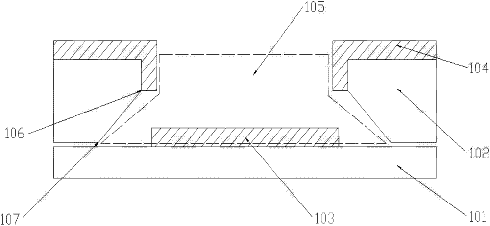
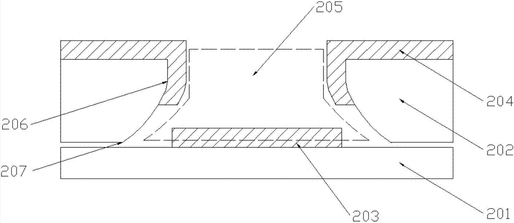
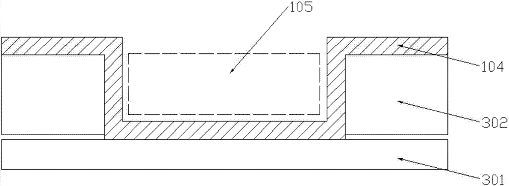
[0027] The present invention aims at the existing OLED thin-film packaging mask, and solves the problem of the prior art OLED thin-film packaging mask, the generation of continuous thin film at the substrate, the mask and the junction of the two, and the rising process of the mask. It is easy to tear and break in the film, thus causing a large number of particles to be generated, and then causing the technical problem of the failure of the thin film package. The embodiment of the present invention can solve this defect.

[0028] Such as figure 1 As shown, the sectional view of the mask plate for OLED thin film encapsulation provided by Embodiment 1 of the present invention, the mask plate for OLED thin film encapsulation provided by the present invention includes: a hollowed out portion, and the hollowed out portion includes a The opening 105 of the layer 103; the cover part 102, the cover part 102 is used to cover the non-thin-film encapsulation area of ​​the substrate 101, ...


PUM


Abstract

The invention provides a mask for encapsulation of an organic light emitting diode (OLED) thin film. The mask comprises a hollow part and a cover part, wherein the hollow part comprises an opening hole used for forming a thin film encapsulation layer on a substrate, the cover part is used for covering a non-film encapsulation region of the substrate, one surface, in contact with the substrate, ofthe cover part is a first surface, one surface, far away from the substrate, of the cover part is a second surface, and at one side, in contact with the substrate, of the cover part arranged around the opening hole, a corner cut is formed at least one part of an edge of the cover part. By the mask, the technical problem that a large amount of particles are generated during raising of the mask to further cause failure of thin film encapsulation due to a continuous thin film generated on the substrate and the mask and at a connection position of the substrate and the mask of the mask for encapsulation of the OLED thin film in the prior art is solved.

Description

technical field [0001] The invention relates to a mask plate, in particular to a mask plate for OLED thin film packaging. Background technique [0002] OLED display is a new generation of display. By making an organic film on an OLED substrate, the organic film is wrapped between the cathode and the anode metal, and a voltage is applied to the two electrodes, and the organic film will emit light. Compared with liquid crystal displays, OLED displays have many advantages such as self-illumination, fast response, wide viewing angle, and saturated colors, including the possibility of curved surface display. For example, using a bendable plastic substrate as a carrier, combined with a thin film packaging process, a bendable OLED panel can be realized. [0003] At present, OLED thin film encapsulation mainly adopts the structure of inorganic layer and organic layer stacking. The inorganic layer materials are commonly used such as SiNx, SiOx, SiON, etc.; the organic layer is commo...

Claims


Application Information

Patent Timeline
Patent Type & Authority Applications(China)
IPC IPC(8): H01L51/52H01L51/56
CPCC23C14/042H10K50/844H10K71/00H10K50/80H10K50/84
Inventor 余威
Owner WUHAN CHINA STAR OPTOELECTRONICS SEMICON DISPLAY TECH CO LTD
Why Eureka
Try Eureka