Method of forming semiconductor device

A semiconductor and device technology, applied in the field of semiconductor device formation, can solve problems such as pattern performance needs to be improved, and achieve the effect of improving performance

Active Publication Date: 2018-01-12
SEMICON MFG INT (SHANGHAI) CORP +1
View PDF2 Cites 5 Cited by
  • Summary
  • Abstract
  • Description
  • Claims
  • Application Information

AI Technical Summary

Problems solved by technology

[0006] However, the performance of patterns in semiconductor devices formed by s

Method used


Image

  • Method of forming semiconductor device
  • Method of forming semiconductor device
  • Method of forming semiconductor device

Examples


Embodiment Construction

[0034] As mentioned in the background, the performance of the pattern in the semiconductor device formed by the self-aligned quadruple patterning technology in the prior art needs to be improved.

[0035] Figure 1 to Figure 5 It is a structural schematic diagram of the formation process of a semiconductor device.

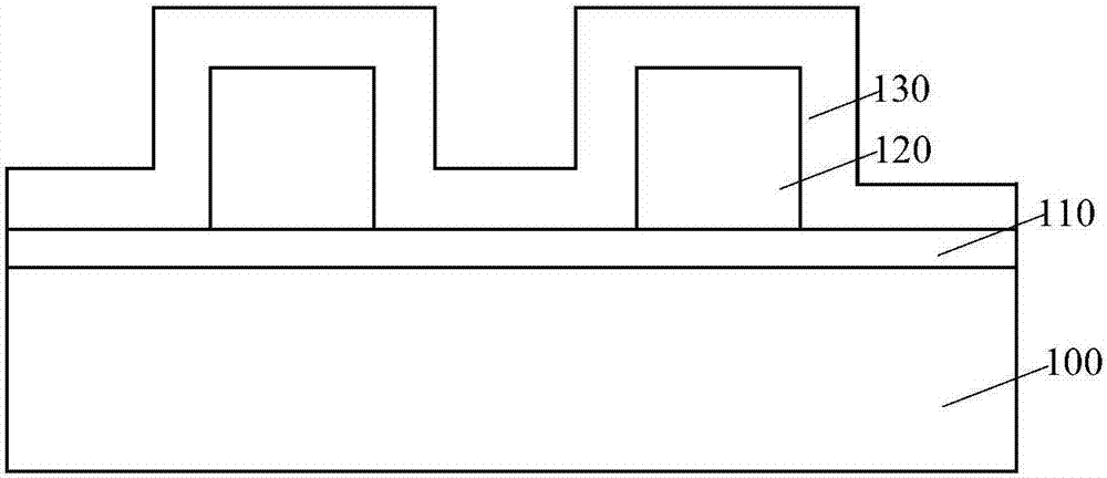
[0036] refer to figure 1, provide the material layer 100 to be etched, the surface of the material layer 100 to be etched has an etching barrier layer 110; a sacrificial layer 120 with a pattern is formed on the surface of the etching barrier layer 110; The first sidewall material layer 130 is formed with the sidewall surface and the surface of the etch stop layer 110 .

[0037] The material of the etch stop layer 110 is silicon nitride.

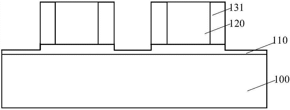
[0038] refer to figure 2 , using an anisotropic dry etching process to etch the first sidewall material layer 130 to form the first sidewall 131 .

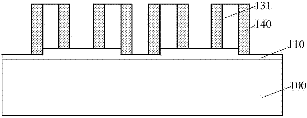
[0039] refer to image 3 , remove the sacrificial layer 120 (refer to f...


PUM

PropertyMeasurementUnit
Thicknessaaaaaaaaaa

Abstract

A method for forming a semiconductor device includes the steps of providing a material layer to be etched, wherein material layer to be etched has a barrier layer; forming a plurality of discrete sacrificial layers on the surface of the barrier layer; forming a first sidewall material layer on the top surfaces and the sidewall surfaces of the sacrificial layers, and the surface of the barrier layer; etching the first sidewall material layer until exposing the surface of the barrier layer and top surfaces of the sacrificial layers, forming a first side wall on the sidewalls of the sacrificial layers, with an etching selection ratio of the first sidewall material layer to the barrier layer being greater than or equal to 10; and after removing the sacrificial layers, etching the barrier layerand the material to be etched by using the first sidewall as a mask. The method of forming the semiconductor device improves the performance of the patterns in the semiconductor device.

Description

technical field [0001] The invention relates to the field of semiconductor manufacturing, in particular to a method for forming a semiconductor device. Background technique [0002] In the manufacturing process of semiconductor devices, the pattern on the mask plate is usually transferred to the substrate by photolithography process. The photolithography process includes: providing a substrate; forming a photoresist on the semiconductor substrate; exposing and developing the photoresist to form a patterned photoresist, so that the pattern on the mask plate is transferred to the photoresist Middle; the substrate is etched with the patterned photoresist as a mask, so that the pattern on the photoresist is transferred to the substrate; the photoresist is removed. With the continuous shrinking of the size of semiconductor devices, the critical dimensions of lithography are gradually approaching or even exceeding the physical limit of lithography, which poses more severe challen...

Claims


Application Information

Patent Timeline
IPC IPC(8): H01L21/336
Inventor 张海洋王彦
Owner SEMICON MFG INT (SHANGHAI) CORP
Why Eureka
Try Eureka