

Embedded substrate
An embedded and substrate technology, which is applied in the direction of electrical components, electric solid devices, circuits, etc., can solve the problems of large chip footprint, limited packaging integration of embedded substrates, and low product reliability, so as to improve packaging integration, The effect of reducing the depth and improving the reliability of the product
- Summary
- Abstract
- Description
- Claims
- Application Information
AI Technical Summary
Problems solved by technology
Method used
Image

Examples
Embodiment Construction
[0046] In order to make the purpose, technical solution and advantages of the application clearer, the application will be further described in detail below in conjunction with the accompanying drawings.
[0047] The present application provides an embedded substrate, which is used to solve the problem that the embedded substrate in the prior art has a large area occupied by all chips and low product reliability, which further limits the further improvement of the package integration of the embedded substrate.
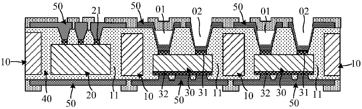
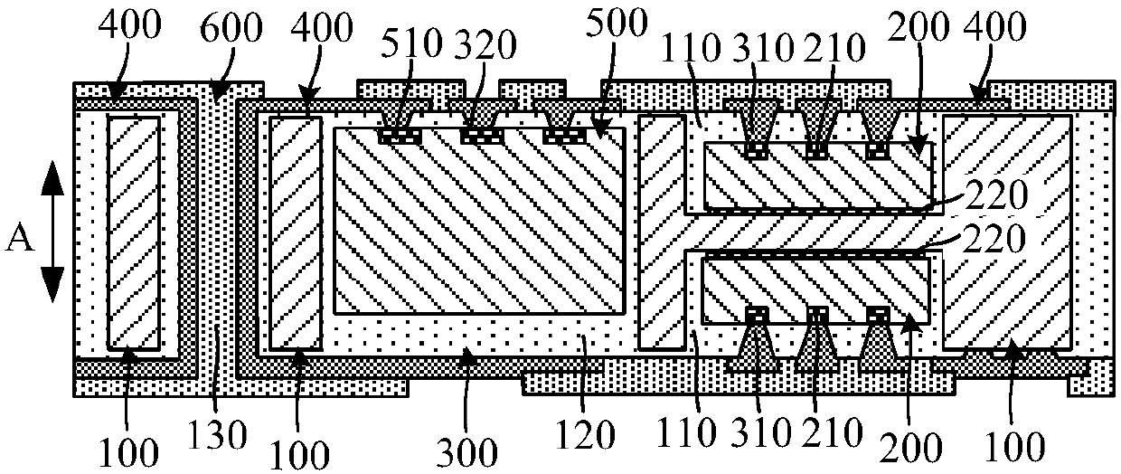
[0048] see figure 2 as shown, figure 2 It is a schematic cross-sectional structure diagram of an embedded substrate provided in an embodiment of the present application, and the embedded substrate includes:
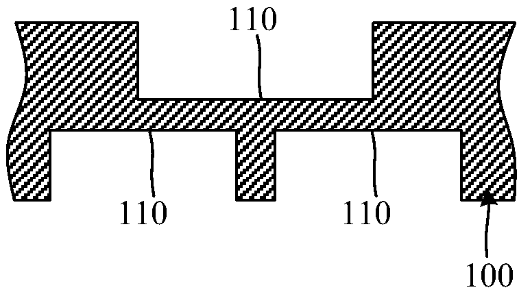
[0049] substrate 100, figure 2 The direction indicated by the middle arrow A is the thickness direction of the substrate 100, and a first chamber 110 is respectively provided on both sides of the substrate 100 in the thickness direction, and the depth of each...
PUM
 Abstract
Description
Claims
Application Information