Wavelength-tunable module

A wavelength, PCB motherboard technology, applied in the coupling of optical waveguides, lasers, instruments, etc., can solve the problems of complex design of tunable modules, high cost, not suitable for mass production of modules, etc., to avoid development costs.

Inactive Publication Date: 2018-01-23
GUANGXUN SCI & TECH WUHAN
View PDF6 Cites 14 Cited by
  • Summary
  • Abstract
  • Description
  • Claims
  • Application Information

AI Technical Summary

Problems solved by technology

[0006] The technical problem to be solved by the present invention is that the existing tunable modules are complex in design, have a long development cycle and high cost, and are not suitable for mass production of modules

Method used


Image

  • Wavelength-tunable module
  • Wavelength-tunable module
  • Wavelength-tunable module

Examples


Embodiment 1

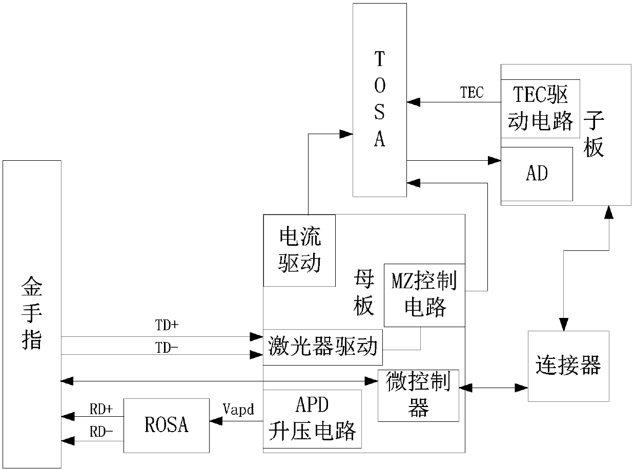
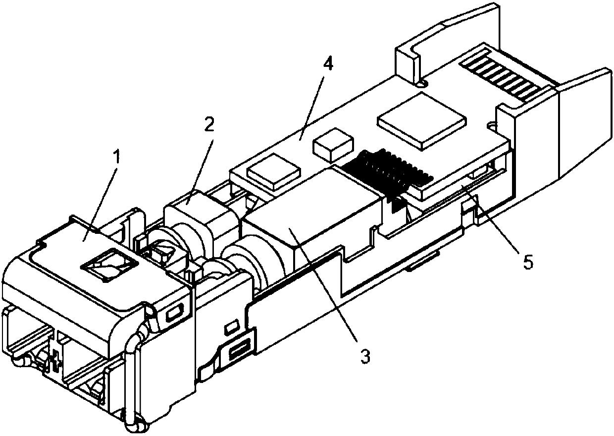
[0056] Such as Figure 1-Figure 6 As shown, Embodiment 1 of the present invention provides a wavelength tunable module, including a housing 1, ROSA2 and TOSA3, and the wavelength tunable module also includes a PCB main board 4 and a PCB sub-board 5, specifically:

[0057] A microcontroller 4-1, an APD boost circuit 4-2, a laser driver 4-3, a gold finger 4-4, a laser current chip 4-5 and a power chip 4-6 are arranged on the PCB main board 4;

[0058] The PCB main board 4 is provided with an interface connected to the data and power supply ports of the ROSA2 and TOSA3;

[0059] For example: the ROSA can be an APD-TIA structure. TIA is built into ROSA, and APD (built into ROSA) has a rate of 10G / bs.

[0060] The PCB sub-board 5 includes a TEC drive circuit 5-1 and a voltage conversion chip 5-4;

[0061] The PCB main board 4 and the PCB sub-board 5 complete the corresponding connection of the power supply channel and the signal channel between the two through pins or flexible c...

Embodiment 2

[0076] After explaining the main structure in Embodiment 1, the embodiment of the present invention will start from the functions of the main structure, explain how the embodiment of the present invention can ensure the work of the tunable module through various functions, and further propose corresponding improvement ideas .

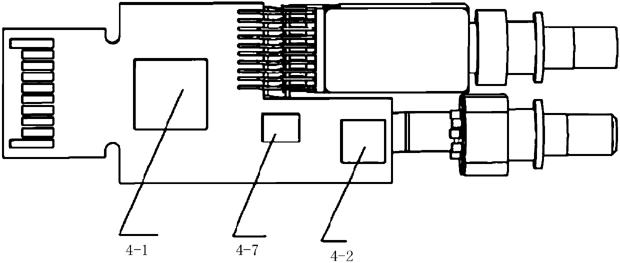
[0077] Such as image 3As shown, it is a front schematic view of the motherboard of the present invention. The motherboard is "L" shaped and includes a microcontroller 4-1 (Renesas 51116ADLF), an operational amplifier 4-7, and a boost chip 4-2 of 508LGGP. The controller 4-1 and the operational amplifier are located on the long side of the "L" shape, and the boost chip is located on the short side of the "L" shape. Figure 4 As shown, it is the back of the motherboard, including a laser driver GN2044S (ie 4-3), a power supply chip 4-6, a current-mode driver MAX5112 chip (ie 4-5), golden fingers 4-4, 2-pin connector 4-8 and 10-pin connectors 4-9. In th...


PUM


Abstract

The invention relates to the technical field of tunable modules and provides a wavelength-tunable module. The wavelength-tunable module comprises a housing 1, an ROSA, a TOSA, a PCB motherboard 4 anda PCB daughter board 5, wherein the PCB motherboard 4 is provided with a microcontroller, an APD boost circuit, a laser driver, a gold finger, a laser current chip and a power supply chip; double-armdifferential modulation is adopted by the laser current chip; an interface is arranged on the PCB motherboard 4 and is connected with data and power supply ports of the ROSA and the TOSA; and the PCBdaughter board 5 comprises a TEC drive circuit and a voltage conversion chip. The miniaturized packaging requirements of the module are achieved through adopting the design of a double-layer circuit board and optimizing the layout mode, thereby avoiding high development cost and a relatively long development cycle caused by special development of an ASIC chip.

Description

【Technical field】 [0001] The invention relates to the technical field of tunable modules, in particular to a wavelength tunable module. 【Background technique】 [0002] At present, in a dense wavelength division multiplexing (Dense Wavelength Division Multiplexing, DWDM for short) system, there are many kinds of wavelengths, which requires optical modules of various wavelengths as light sources. In order to ensure the reliability and stability of the communication system, each optical module requires at least one backup module of the same wavelength, which brings problems such as low resource utilization, complex module management, poor flexibility of optical network nodes, and high network construction costs. . [0003] Since the 21st century, due to the explosive growth of Internet services, the world's demand for network bandwidth is increasing day by day. The development of optical fiber communication network as information bearing and transmission presents two obvious ...

Claims


Application Information

Patent Timeline
IPC IPC(8): H01S5/042G02B6/42G02B6/293
Inventor 成璇璇胡毅宋耕
Owner GUANGXUN SCI & TECH WUHAN
Why Eureka
Try Eureka