GaN technological parameter statistical analysis method based on large signal equivalent circuit model

A technology of equivalent circuit model and process parameters, applied in electrical digital data processing, instruments, calculations, etc., can solve problems such as insufficient accuracy, affecting the yield of circuit design, fluctuations in process parameters, etc., and achieve the effect of improving accuracy

Active Publication Date: 2018-01-26
UNIV OF ELECTRONICS SCI & TECH OF CHINA
View PDF3 Cites 7 Cited by
  • Summary
  • Abstract
  • Description
  • Claims
  • Application Information

AI Technical Summary

Problems solved by technology

[0003] However, due to unintentional doping and process parameter fluctuations in the device preparation process, it will affect the consistency of device performance, thereby affecting the yield of circuit design, so it is necessary to guide the analysis of circuit yield by establishing a statistical model
Traditional statistical methods are based on the small signal model or some large signal model parameters, so the accuracy is insufficient
Moreover, it is impossible to obtain specific statistical analysis of process parameters through large-signal statistical models to guide device yield design and process parameter optimization

Method used


Image

  • GaN technological parameter statistical analysis method based on large signal equivalent circuit model
  • GaN technological parameter statistical analysis method based on large signal equivalent circuit model
  • GaN technological parameter statistical analysis method based on large signal equivalent circuit model

Examples


Embodiment Construction

[0047] The following will clearly and completely describe the technical solutions in the embodiments of the present invention with reference to the accompanying drawings in the embodiments of the present invention. Obviously, the described embodiments are only some, not all, embodiments of the present invention. Based on the embodiments of the present invention, all other embodiments obtained by persons of ordinary skill in the art without making creative efforts belong to the protection scope of the present invention.

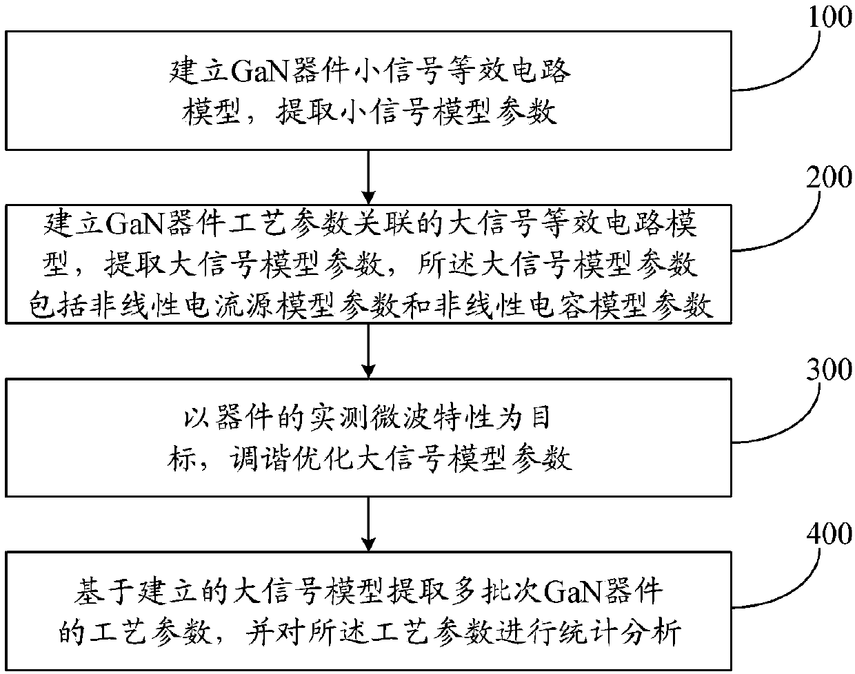
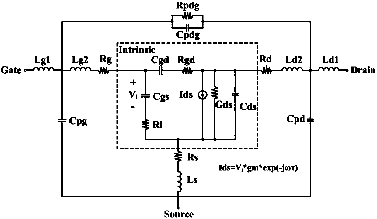
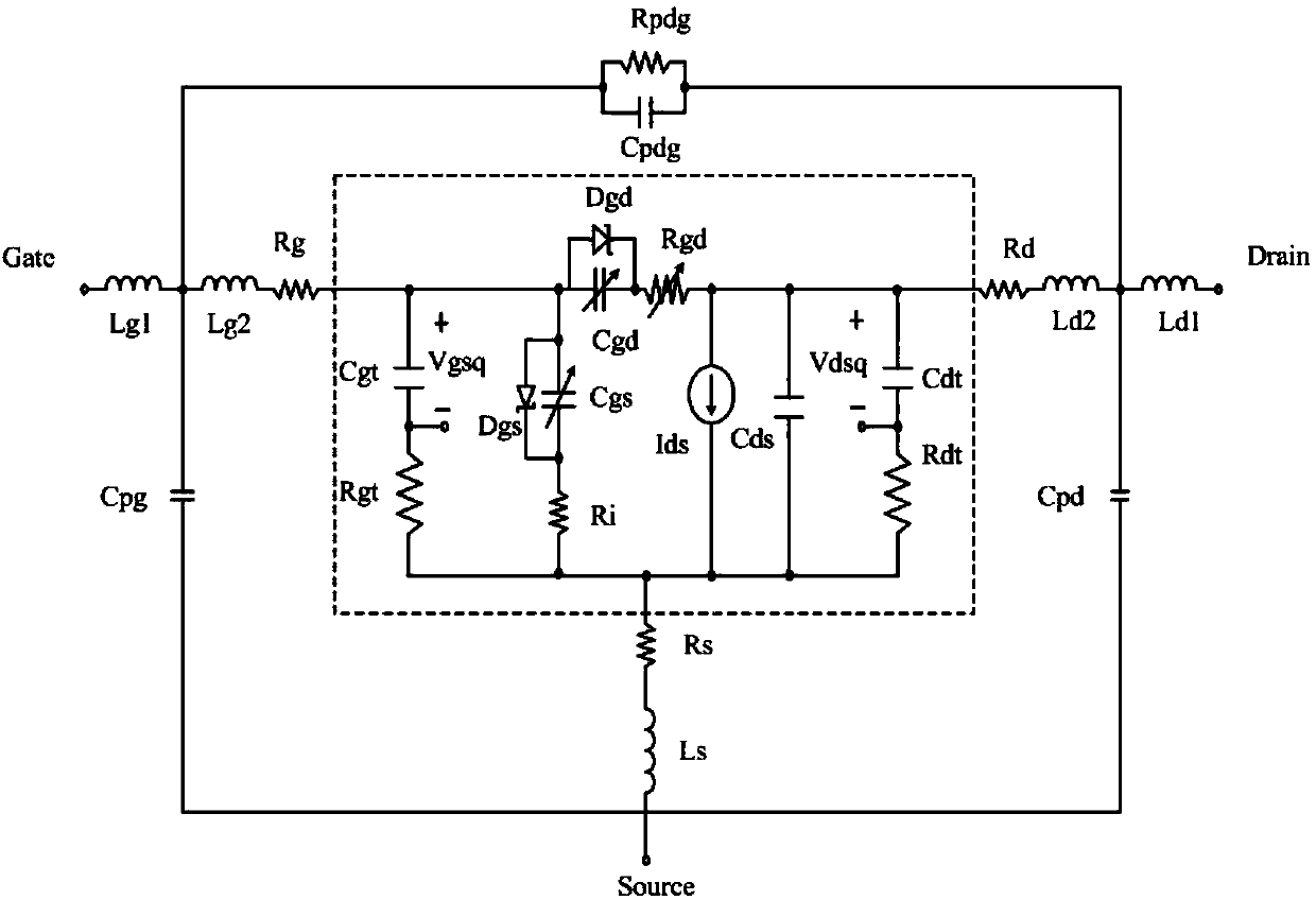
[0048] The purpose of the present invention is to provide a GaN device process parameter statistical analysis method based on a large-signal equivalent circuit model. First, a GaN device small-signal equivalent circuit model is established, and then a GaN device large-signal equivalent circuit model associated with physical parameters is established. Finally, the statistical characteristics of the process parameters are obtained, which can effectively analyze t...


PUM


Abstract

The invention provides a GaN technological parameter statistical analysis method based on large signal equivalent circuit model. The analysis method comprises the following steps: a step 1: establishing a GaN device small signal equivalent circuit model, and extracting small signal model parameters; a step 2: establishing a GaN device large signal equivalent circuit model, and extracting large signal model parameters, that is non-linear current source model parameter and non-linear capacitance model parameter; a step 3: actually measured microwave characteristics of the device are used as objects in order to tune and optimize large signal model parameters; a step 4: extracting multiple-batch GaN device technological parameters based on established large signal model, and carrying out statistical analysis of the technological parameters. The GaN device model technological parameter statistical analysis method firstly establishes the GaN device small signal equivalent circuit model, andthen establishes GaN device large signal equivalent circuit model related to technological parameters, finally technological parameter statistical distribution is obtained by multiple-bath device modeling, and the method is good for device yield analysis and technological parameter optimization.

Description

technical field [0001] The invention relates to the technical field of GaN HEMT (gallium nitride high electron mobility transistor) devices, in particular to a statistical analysis method for GaN device process parameters based on a large-signal equivalent circuit model. Background technique [0002] Gallium Nitride High Electron Mobility Transistor (GaNHEMT) has extremely important applications in microwave and millimeter wave solid-state power circuits due to its high frequency and high power density. The current mainstream method of circuit design is usually based on the device model that describes the characteristics of the device under small-signal working conditions and large-signal working conditions in the form of an equivalent circuit, so the device model is the premise of using the device for circuit design. [0003] However, due to unintentional doping and process parameter fluctuations in the device preparation process, it will affect the consistency of device pe...

Claims


Application Information

Patent Timeline
Patent Type & Authority Applications(China)
IPC IPC(8): G06F17/50
CPCG06F2111/08G06F30/367G06F2111/10
Inventor 徐跃杭闻彰徐锐敏延波
Owner UNIV OF ELECTRONICS SCI & TECH OF CHINA
Why Eureka
Try Eureka