Method for forming insulating groove in substrate and semiconductor device

A technology of insulating trenches and semiconductors, which is applied in the manufacture of semiconductor/solid-state devices, electrical components, circuits, etc., and can solve the problems of increasing the manufacturing cost of semiconductor devices with insulating trenches, high manufacturing costs, and complicated processes

Inactive Publication Date: 2018-02-02
GLOBAL ENERGY INTERCONNECTION RES INST CO LTD +2
View PDF4 Cites 0 Cited by
  • Summary
  • Abstract
  • Description
  • Claims
  • Application Information

AI Technical Summary

Problems solved by technology

In the technical solution adopted in the Chinese patent application CN106409898A, although the post-implantation of high-energy oxygen ions to thicken the bottom oxide layer can effectively reduce the peak value of the electric field at the corner of the trench, however, injecting high-ener

Method used


Image

  • Method for forming insulating groove in substrate and semiconductor device
  • Method for forming insulating groove in substrate and semiconductor device
  • Method for forming insulating groove in substrate and semiconductor device

Examples


Embodiment Construction

[0028] The technical solutions of the present invention will be clearly and completely described below in conjunction with the accompanying drawings. Apparently, the described embodiments are some of the embodiments of the present invention, but not all of them. Based on the embodiments of the present invention, all other embodiments obtained by persons of ordinary skill in the art without making creative efforts belong to the protection scope of the present invention. In addition, the terms "first", "second", etc. are used for descriptive purposes only, and should not be construed as indicating or implying relative importance.

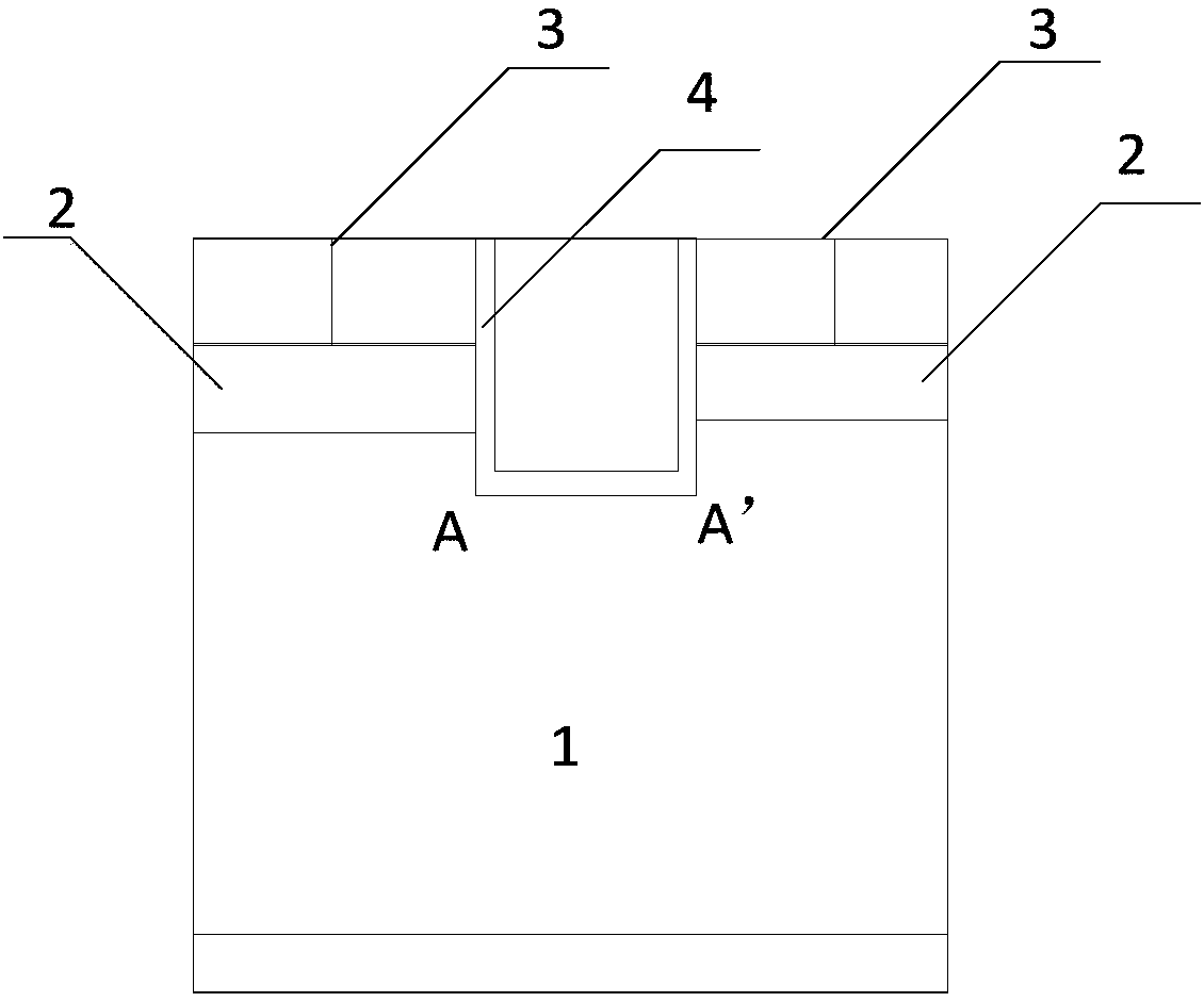
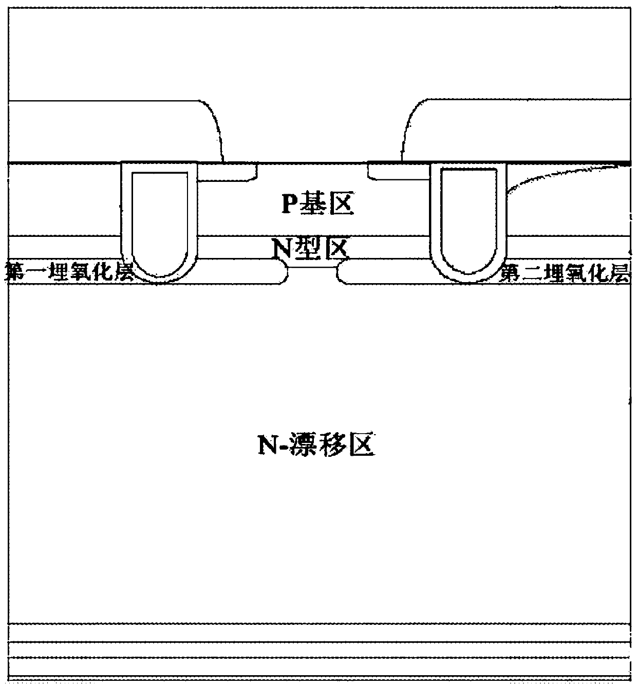
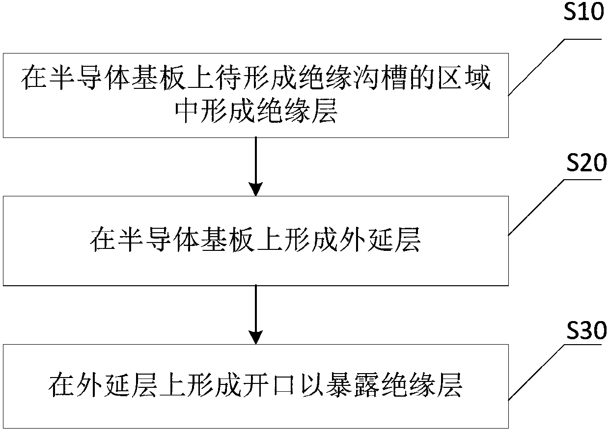
[0029] An embodiment of the present invention provides a method for forming an insulating trench on a substrate, such as image 3 As shown, the method includes:

[0030] S10 . Form an insulating layer 20 in a region on the substrate 10 where the insulating trench 40 is to be formed. In a specific embodiment, the substrate 10 may be a silicon substra...


PUM


Abstract

The invention provides a method for forming an insulating groove in a substrate and a semiconductor device. The method comprises the steps as follows: an insulating layer is formed in the region, in which an insulating groove is to be formed, on the surface of a substrate, wherein the insulating layer can be taken as the bottom of the insulating groove, the specific thickness can be correspondingly adjusted according to the device type and the operating requirements, forming of the insulating layer on the surface of the substrate is relatively easy to implement, and the thickness and the region range are relatively easy to control; an epitaxial layer is formed on the substrate, and the structure of the epitaxial layer can be determined according to the type of the semiconductor device; andan opening is formed in the epitaxial layer to expose the insulating layer, thereby forming the insulating groove. Compared with the prior art, the method has the advantages that control on the thickness of the bottom of the insulating layer at the bottom of the groove and improvement of electric field distribution can be implemented, additional equipment or process is not needed for implementation, and the implementation procedure and the implementation process are simple.

Description

technical field [0001] The invention relates to the technical field of chip manufacturing, in particular to a method for forming an insulating trench on a substrate and a semiconductor device. Background technique [0002] The importance of power semiconductor devices has become increasingly prominent under the continuous and rapid growth of energy demand, and they are widely used in switching power supplies, automotive electronics, new energy, power transmission and transformation, rail transit, metallurgy and chemical industries. [0003] Power semiconductor devices are usually used as switches, and their on-resistance and breakdown voltage are two key parameters. Reducing the on-resistance can reduce the dynamic and static loss of the device and increase the switching speed. Therefore, generally, the trench gate structure is used to reduce the on-resistance of the device, of which figure 1 An exemplary structural diagram of a trench gate semiconductor is shown. The proce...

Claims


Application Information

Patent Timeline
IPC IPC(8): H01L21/762
CPCH01L21/76224H01L21/76237
Inventor 刘江朱涛金锐李立王耀华温家良潘艳
Owner GLOBAL ENERGY INTERCONNECTION RES INST CO LTD
Why Eureka
Try Eureka