Heat dissipation structure of high speed optical module

A heat dissipation structure and optical module technology, applied in the field of optical modules, can solve the problems of affecting the high temperature performance of the module, unfavorable rapid heat dissipation of the module, and unscientific heat dissipation paths, and achieve the effect of improving high temperature performance, reducing working power consumption, and improving heat dissipation function.

Inactive Publication Date: 2018-02-06
WUHAN TELECOMM DEVICES
View PDF1 Cites 8 Cited by
  • Summary
  • Abstract
  • Description
  • Claims
  • Application Information

AI Technical Summary

Problems solved by technology

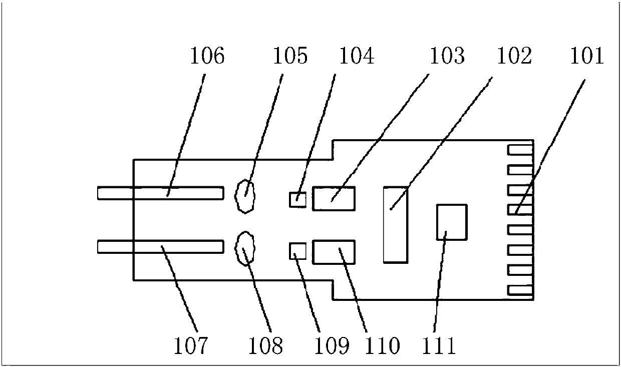
However, according to the requirements of the agreement, in the actual application of this module, the heat dissipation area of ​​the external system is also distributed on the top layer, such as Figure 4 As shown, most of the current PAM chip 102, laser driver chip 103, and transimpedance amplifier chip / limiting amplifier 110 are positive-mounted chips (that is, the top layer of the chip is used for gold wire bonding to realize electrical connection, and the bottom layer of the chip is used for SMD, fixed on the carrier board, and conduct heat dissipation through the bottom contact), that is to say, this kind of electric chip needs to be dissipated from the bottom layer, and the bottom layer is close to the direction of the test circuit board, and is suspended, so the existing module The heat dissipation design is not conducive to the rapid heat dissipation of the module in a high temperature environment. The main heat of the module is first dissipated to the bottom layer of the shell, and then uploaded to the top layer of the shell through the side wall of the shell, and then dissipated through the heat dissipation area of ​​the external system
This heat dissipation path is not scientific enough, which affects the high temperature performance of the module
When the total power consumption of the module is low, the impact is not obvious, but for PAM4-based optical modules with high power consumption, heat dissipation is a major problem

Method used


Image

  • Heat dissipation structure of high speed optical module
  • Heat dissipation structure of high speed optical module
  • Heat dissipation structure of high speed optical module

Examples


Embodiment 1

[0045] Embodiment 1 of the present invention provides a heat dissipation structure of a high-speed optical module, such as Image 6 with Figure 8 As shown, it includes a tube shell base 214, a cover plate 215 and a light engine. The heat dissipation structure also includes a PCB bottom plate 213, a first Z-shaped transition plate 212 and a gold finger sub-board 201, specifically:

[0046] An electrical signal connection is established between the PCB bottom plate 213 and the golden finger sub-board 201 through the first Z-shaped transition plate 212; wherein, the first Z-shaped transition plate 212 enables the PCB bottom plate 213 to be fixed to the After the package base 214, the first surface 2131 of the PCB base plate 213 is adjacent to the bottom of the package base 214, and the second surface 2132 on the PCB base plate 213 with the light engine faces the cover 215 side of the optical module;

[0047] Wherein, the length of the gold finger sub-board 201 is set according to the ...


PUM


Abstract

The invention relates to the technical field of optical modules and provides a heat dissipation structure of a high speed optical module. Electrical signal connection is established between a PCB baseplate 213 and a gold finger auxiliary plate 201 through a first Z-shaped transition plate 212. After the first Z-shaped transition plate 212 fixes the PCB base plate 213 on a pipe case base 214, thefirst surface 2131 of the PCB base plate 213 is adjacent to the bottom of the pipe case base 214 and the second surface 2132 equipped with an optical engine on the PCB base plate 213 faces the cover plate 215 side of the optical module. According to the invention, in the design of the optical module, space layout at the bottom of the module is adjusted, so the optical engine which produces heat severely and is quite high in power consumption is partially designed to be mounted to the base layer of the PCB base plate or a bearing substrate; heat dissipation through the top layer of the module is facilitated; the heat dissipation structure can directly cooperate with the heat dissipation device of an external application system; heat dissipation functions of the module are improved; workingpower consumption is reduced; and high temperature performance of the whole optical module is improved.

Description

【Technical Field】 [0001] The present invention relates to the technical field of optical modules, in particular to a heat dissipation structure of a high-speed optical module. 【Background technique】 [0002] Such as figure 1 As shown, the general structure of the existing high-speed optical module 100 is as follows: Currently, it is divided into a transmitting end and a receiving end. The interface unit 101 receives the NRZ signal or PAM4 signal sent by the system, and converts the NRZ signal to the PAM4 model through the PAM electrical chip 102. Encoding, if the received PAM4 signal is directly encoded, it will be directly encoded and sent to the emission driver 103. The emission driver 103 outputs a current signal or voltage signal to the laser 104. The laser 104 is excited by the light and emits a modulated light signal. The optical signal is transmitted through the transmitting end optical lens 105 and the transmitting fiber port 106, and the optical signal with modulated wav...

Claims


Application Information

Patent Timeline
Patent Type & Authority Applications(China)
IPC IPC(8): G02B6/42
CPCG02B6/4272
Inventor 曹芳付永安高繁荣孙莉萍
Owner WUHAN TELECOMM DEVICES
Why Eureka
Try Eureka