Etching device and etching method for reducing side erosion angle of circuit board

An etching device and circuit board technology, which is applied in chemical/electrolytic methods to remove conductive materials, printed circuits, printed circuit manufacturing, etc., can solve problems affecting the precise wiring of circuit boards, achieve high integration, improve wiring accuracy and Density, the effect of reducing the degree of side erosion

Active Publication Date: 2020-03-31
CHANGSHU MUTUAL TEK CO LTD
View PDF5 Cites 0 Cited by
  • Summary
  • Abstract
  • Description
  • Claims
  • Application Information

AI Technical Summary

Problems solved by technology

[0008] Still another object of the present invention is to provide an etching device and an etching method for reducing the inclination angle of side erosion of a circuit board. The protective sleeve is used to reduce the degree of attack of the side wall of the conductive circuit by the etching solution, and to solve the problem of serious side erosion. Technical Problems of Circuit Board Precise Wiring

Method used


Image

  • Etching device and etching method for reducing side erosion angle of circuit board
  • Etching device and etching method for reducing side erosion angle of circuit board
  • Etching device and etching method for reducing side erosion angle of circuit board

Examples


Embodiment 1

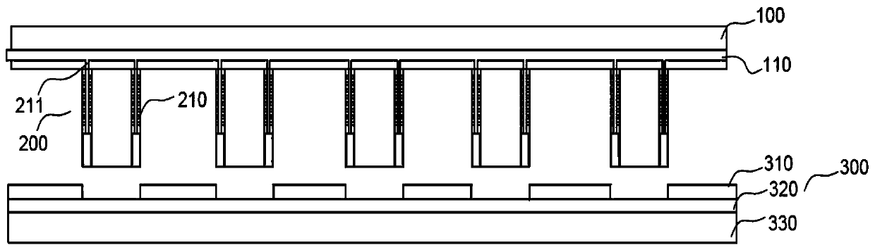
[0036] The invention provides an etching device for reducing the inclination angle of side erosion of a circuit board, such as Figure 1-4 As shown, it includes a mask plate, a press plate 100 and a protective sleeve 200, wherein the mask plate is movably arranged on the upper end of the circuit board 300 to be etched, and is used to mask the photoresist on the circuit board 300, and the mask plate The stencil is provided with a number of through holes. After masking, exposure, and development, the photoresist 310 in the corresponding area of ​​the through holes is removed to expose the part of the conductor to be etched, and then the exposed conductor is etched, and the remaining conductor That is the conductive line.

[0037] The pressing plate 100 is movably arranged on the upper end of the mask plate. After the masking is completed, the mask plate can be removed, and the mask plate can be kept in place. A first channel 110 is arranged laterally in the pressing plate 100 . ...

Embodiment 2

[0045] An etching method of an etching device for reducing the side erosion inclination of a circuit board 300, comprising the following steps:

[0046] Step 1, apply photoresist on the conductive layer of the circuit board 300 to be etched, dry, mask, expose, develop, and show the channel of the photoresist, that is, expose the conductive layer to be etched;

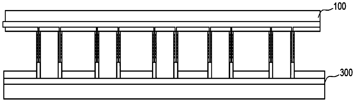
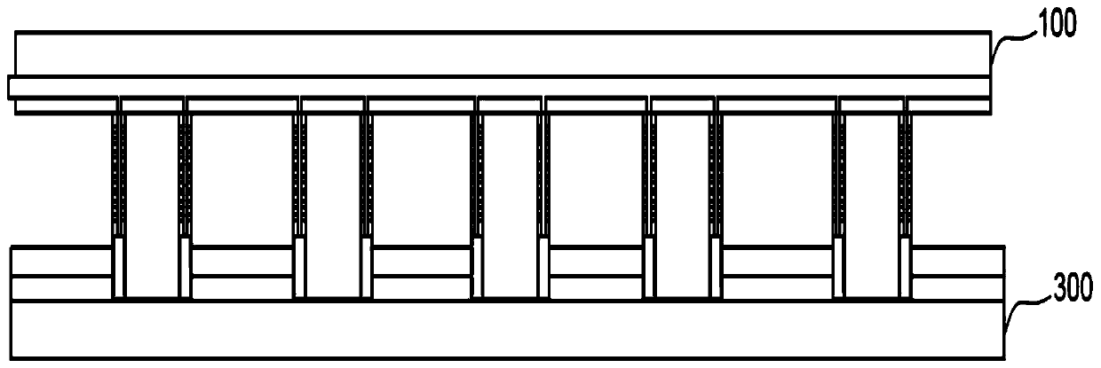
[0047] Step 2: According to the shape and position of the through hole of the mask plate, assemble each side plate 210 at the bottom of the platen 100, so that the shape and position of each protective sleeve 200 are consistent with the shape and position of the through hole of the mask plate, and one through hole corresponds to A protective sleeve 200 with the same shape and location;

[0048] Step 3. The mask can be removed or kept in place, and the platen 100 can be moved laterally to align each of the protective sleeves 200 with the through holes on the mask and the holes on the photoresist. The channels are aligne...


PUM


Abstract

The invention discloses an etching device and method for reducing a side-etching tilt angle of a circuit board. The etching device comprises a mask plate which is movably arranged at the upper end ofthe circuit board, and is provided with a plurality of through holes, a pressure plate which is movably arranged at the upper end of the mask plate, and is internally and transversely provided with afirst channel of which an inlet is communicated with a container with an etching liquid, and a protective sleeve which is of a cylindrical structure having a cross section and is coincident with the cross section of the through hole, wherein the upper end of the protective sleeve is connected with the bottom of the pressure plate, and the protective sleeve is formed by splicing a plurality of sideplates; a hollow cavity is arranged in the bottom of the side plate, and a second channel is longitudinally arranged at the upper part of the side plate; and the second channel is communicated with the first channel and the hollow cavity, and a plurality of side holes are formed in the upper end of each side plate in a penetrating way. The etching device and method provided by the invention solvethe technical problem that the precise wiring of the circuit board is affected due to severe side-etching.

Description

technical field [0001] The invention relates to the technical field of circuit board preparation, more specifically, the invention relates to an etching device and an etching method for reducing the side erosion angle of a circuit board. Background technique [0002] Today is the era of communication, fast, light, multi-tasking and high quality are the most basic functions of related electronic or optoelectronic products, so the design and manufacture of related products must be oriented towards light, thin, multi-functional, fast, and low price direction of development. [0003] Based on this, High Density Interconnect (HDI) substrates with thin lines and tiny holes as a function of carrying assembly functions will emerge as the times require, and the demand for circuit miniaturization technology will become increasingly urgent, and the quality control requirements will also increase. It is becoming more and more stringent, which means that when the line width and line spa...

Claims


Application Information

Patent Timeline
Patent Type & Authority Patents(China)
IPC IPC(8): H05K3/06
CPCH05K3/061H05K3/068H05K2203/0557
Inventor 赖文钦陈秋予邱士于
Owner CHANGSHU MUTUAL TEK CO LTD
Why Eureka
Try Eureka