Multi-layer circuit board and fabrication method of same

A multi-layer circuit board and core board technology, which is applied in multi-layer circuit manufacturing, printed circuit manufacturing, printed circuit, etc., can solve the problem of reducing the success rate of circuit board stacking and lamination once Problems such as normal production can be solved to achieve the effect of reducing punching and repeated alignment processes, improving precision, improving production efficiency and production quality

Active Publication Date: 2018-02-16
NEW FOUNDER HLDG DEV LLC +1
View PDF10 Cites 7 Cited by
  • Summary
  • Abstract
  • Description
  • Claims
  • Application Information

AI Technical Summary

Problems solved by technology

[0002] In the related art, in order to reduce the production cost of multilayer circuit boards and shorten the production cycle of multilayer circuit boards, a circuit board design method of combining multiple core boards is used to prepare circuit boards. Taking the combination of two core boards as an example, Compared with the traditional preparation method, it can reduce one pressing process, one drilling process and one electroplating process, and use fusion alignment combination process instead of rivet combination process. While it has technical advantages and cost advantages, it also has certain defects. The existing fusion alignment combination process uses a double-hole concentric circle alignment system. The double-hole concentric circle alignment system aligns the PIN holes on the punched circuit board. The alignment method is to grab the PIN holes. Outline, the system alignment hole of the fusion machine coincides with the outline of the PIN hole on the circuit board to complete the combined alignment. This alignment method needs to go through graphic line alignment and punching alignment. The accumulated deviation value of multiple alignments will affect the product. quality, and the alignment method is affected by many factors such as the overall expansion and contraction of the product, the roundness of the PIN hole, and the quality of the PIN hole. It is necessary to repeatedly grab the contour of the PIN hole, and when the contours of the two alignment holes are inconsistent, the alignment will not be possible, resulting in failure of normal production, thereby reducing the first-time success rate of circuit board stacking and pressing and the production efficiency of circuit boards

Method used


Image

  • Multi-layer circuit board and fabrication method of same
  • Multi-layer circuit board and fabrication method of same
  • Multi-layer circuit board and fabrication method of same

Examples


Embodiment Construction

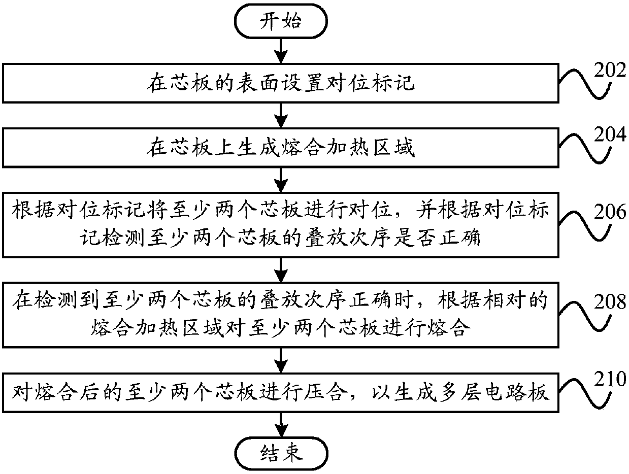
[0035]In order to understand the above-mentioned purpose, features and advantages of the present invention more clearly, the present invention will be further described in detail below in conjunction with the accompanying drawings and specific embodiments. It should be noted that, in the case of no conflict, the embodiments of the present application and the features in the embodiments can be combined with each other.

[0036] In the following description, many specific details are set forth in order to fully understand the present invention. However, the present invention can also be implemented by a third party different from the third party described here. Therefore, the protection scope of the present invention is not limited by the following disclosure. The limitations of specific examples.

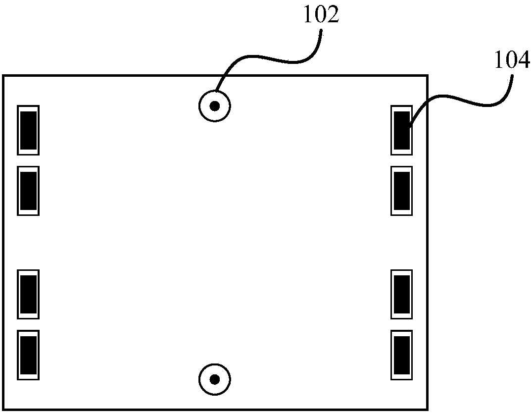
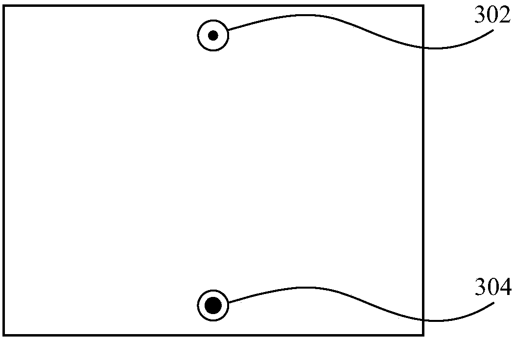
[0037] figure 1 A schematic diagram of a multilayer circuit board according to an embodiment of the present invention is shown.

[0038] Such as figure 1 As shown, the multilayer ...


PUM


Abstract

The invention provides a multi-layer circuit board and a fabrication method of the same. The multi-layer circuit board comprises at least two optical alignment marks and at least two melting heating regions, wherein the at least two optical alignment marks are arranged on core boards by etching and are used for aligning at least two core boards, and the at least two melting heating regions are arranged on board edges of the core boards and are used for melting after the alignment of the at least two core boards is completed. By the technical scheme, the punching and repeated alignment processis reduced, abnormal alignment caused by an abnormal factor such as alignment hole deformation is prevented, the alignment accuracy is improved, and the production efficiency and the production quality of the circuit board are improved.

Description

technical field [0001] The invention relates to the technical field of circuit boards, in particular to a multilayer circuit board and a method for preparing the multilayer circuit board. Background technique [0002] In the related art, in order to reduce the production cost of multilayer circuit boards and shorten the production cycle of multilayer circuit boards, a circuit board design method of combining multiple core boards is used to prepare circuit boards. Taking the combination of two core boards as an example, Compared with the traditional preparation method, it can reduce one pressing process, one drilling process and one electroplating process, and use fusion alignment combination process instead of rivet combination process. While it has technical advantages and cost advantages, it also has certain defects. The existing fusion alignment combination process uses a double-hole concentric circle alignment system. The double-hole concentric circle alignment system al...

Claims


Application Information

Patent Timeline
Patent Type & Authority Applications(China)
IPC IPC(8): H05K1/02H05K3/46
CPCH05K1/02H05K1/0269H05K3/4611H05K3/4638H05K2201/09918H05K2201/20H05K2203/065
Inventor 车世民李晋峰陈德福李亮汪汇东
Owner NEW FOUNDER HLDG DEV LLC
Why Eureka
Try Eureka