Manufacturing method of PCB and PCB

A manufacturing method and a stepped technology, which is applied in printed circuit manufacturing, multi-layer circuit manufacturing, printed circuit, etc., can solve the problem of low wiring density, achieve the effect of increasing wiring density and reducing the number of vias

Inactive Publication Date: 2018-02-16
DONGGUAN SHENGYI ELECTRONICS
View PDF4 Cites 2 Cited by
  • Summary
  • Abstract
  • Description
  • Claims
  • Application Information

AI Technical Summary

Problems solved by technology

[0003] The purpose of the present invention is to provide a PCB manufacturing method and PCB, to overcome the defects of low product wiring density existing in the prior art

Method used


Image

  • Manufacturing method of PCB and PCB
  • Manufacturing method of PCB and PCB
  • Manufacturing method of PCB and PCB

Examples


Embodiment Construction

[0028] In order to make the objectives, features, and advantages of the present invention more obvious and understandable, the technical solutions in the embodiments of the present invention will be described clearly and completely in conjunction with the accompanying drawings in the embodiments of the present invention. Obviously, the following The described embodiments are only a part of the embodiments of the present invention, rather than all the embodiments. Based on the embodiments of the present invention, all other embodiments obtained by those of ordinary skill in the art without creative work shall fall within the protection scope of the present invention.

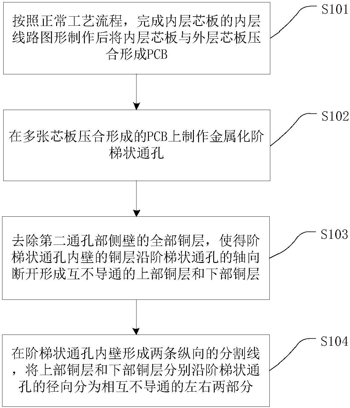
[0029] See figure 1 , figure 1 Shows the PCB manufacturing method flow.

[0030] In this embodiment, the PCB manufacturing method includes the following steps:

[0031] S101. According to the normal process flow, after the inner layer circuit pattern of the inner layer core board is made, the inner layer core board and...


PUM


Abstract

The invention discloses a manufacturing method of a PCB and a PCB. The manufacturing method includes: an inner circuit pattern is manufactured at an inner core plate and then the processed inner coreplate is pressed with an outer core plate to form a PCB; a step-shaped through hole is formed in the PCB and plated-through-hole electroplating is carried out on the through hole, wherein the step-shaped through hole includes a first through hole portion and a second through hole portion in an axial direction and the aperture of the first through hole portion is larger than that of the second through hole portion; and the copper layer of the inner wall of the stepped through hole is broken along the radial direction of the step-shaped through hole to form at least two parts not in conduction.According to the invention, the copper layer of the inner wall of the stepped through hole of the PCB is divided into four parts not in conduction by two-times disconnection and each part of copper layer serves as a network connection layer separately, so that four network connection layers is realized by one step-shaped through hole. Therefore, the via hole number is reduced and the wiring density of the PCB is improved.

Description

Technical field [0001] The present invention relates to the technical field of PCB (Printed Circuit Board, printed circuit board), in particular to a manufacturing method of a PCB and a PCB. Background technique [0002] With the development of high-density integrated circuit technology and microelectronics technology, the volume of electronic products has become lighter, thinner, and smaller. At present, in the design of high-multilayer PCB production and wiring, the network connections between different layers all use vias, and usually only one network connection layer is designed for a via. Since each via occupies a certain area on the PCB board, the larger the PCB capacity, the more the design network, the more the number of vias, and the larger the design area of ​​the PCB board, which cannot meet the needs of thinner electronic products. Smaller requirements. Summary of the invention [0003] The purpose of the present invention is to provide a PCB manufacturing method and...

Claims


Application Information

Patent Timeline
Patent Type & Authority Applications(China)
IPC IPC(8): H05K3/42H05K3/46H05K1/11
CPCH05K3/429H05K1/115H05K3/4611H05K2201/09645
Inventor 王小平纪成光何思良陈正清金侠刘梦茹
Owner DONGGUAN SHENGYI ELECTRONICS
Why Eureka
Try Eureka