High-throughput four-point-probe in-situ resistance measuring equipment for material chips
A technology of in-situ resistance and measurement equipment, applied in the direction of material resistance, etc., can solve the problems of in-situ measurement and recording, difficulty in coping with rapid resistance changes, long measurement intervals, etc., and achieve simple and convenient experimental assembly and connection process, interface Friendly, Inexpensive Effects
- Summary
- Abstract
- Description
- Claims
- Application Information
AI Technical Summary
Problems solved by technology
Method used
Image
Examples
Embodiment 1
[0037] In this embodiment, a high-throughput method is used to screen a component with the smallest resistance temperature effect from a certain ternary material as an example to illustrate the research application of high-throughput in-situ resistance testing equipment. The concrete steps of this embodiment are as follows:
[0038] A1, choose the one prepared by the combined chip method, use a 3-inch quartz plate as the substrate, and coat the surface with 64 independent and different components of a certain ternary material film with a size of A×A (A=1~3mm). sample. Put it into the sample rack, adjust the position and fix it.
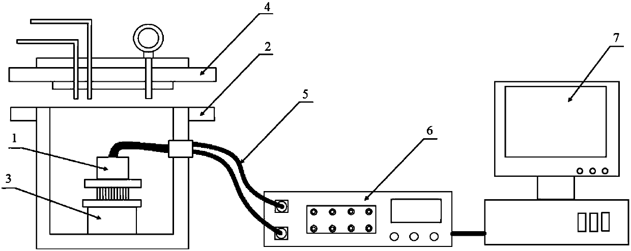
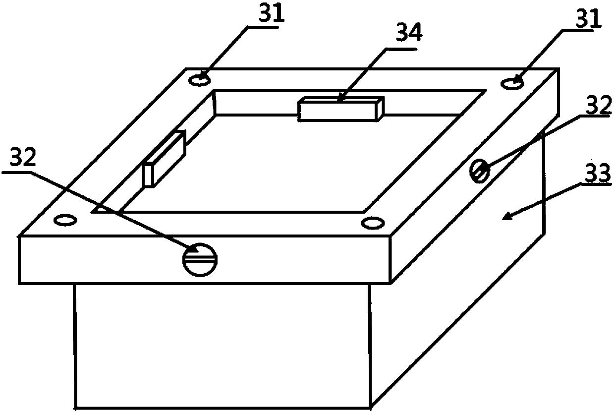
[0039] B1, the high-throughput four-probe probe is fixed to the sample holder with bolts. Since the sample preparation and the design of the probe adopt compatible dimensions, the probe tip of the probe can be in good contact with the appropriate position on the sample surface at this time.
[0040] C1, connect the cable plug of the four-probe probe...
Embodiment 2
[0048] In this embodiment, a high-throughput method is used to screen a component with the fastest hydrogen-sensing resistance response from certain ternary hydrogen-sensitive materials as an example to illustrate the research and application of high-throughput in-situ resistance testing equipment. The concrete steps of this embodiment are as follows:
[0049] A2, choose a 3-inch quartz plate prepared by the combination chip method, and the surface is coated with 64 ternary material films with a size of B×B (A=1~3mm) that are independent of each other and have different compositions. sample. Put it into the sample rack, adjust the position and fix it.
[0050] B2, the high-throughput four-probe probe is fixed to the sample holder with bolts. Since the sample preparation and the design of the probe adopt compatible dimensions, the probe tip of the probe can be in good contact with the appropriate position on the sample surface at this time.
[0051] C2, connect the cable plug...
PUM
 Abstract
Description
Claims
Application Information
 - R&D
- Intellectual Property
- Life Sciences
- Materials
- Tech Scout
- Unparalleled Data Quality
- Higher Quality Content
- 60% Fewer Hallucinations
Browse by: Latest US Patents, China's latest patents, Technical Efficacy Thesaurus, Application Domain, Technology Topic, Popular Technical Reports.
© 2025 PatSnap. All rights reserved.Legal|Privacy policy|Modern Slavery Act Transparency Statement|Sitemap|About US| Contact US: help@patsnap.com


