Double-sided circuit board testing device

A double-sided circuit board and testing device technology, applied in the direction of electronic circuit testing, measuring devices, measuring electricity, etc., can solve the problems of high labor intensity, many working hours, low production efficiency, etc., to reduce the operation process, reduce production costs, The effect of improving productivity

Inactive Publication Date: 2018-02-23
GUANGDONG FEIKETE ELECTRONICS TECH CO LTD
View PDF5 Cites 1 Cited by
  • Summary
  • Abstract
  • Description
  • Claims
  • Application Information

AI Technical Summary

Problems solved by technology

Because the automatic detection system of printed circuit boards in foreign countries is too expensive, and the automatic detection equipment of printed circuit boards in the true sense has not been developed in China, most domestic circuit board manufacturers still use manual inspection with a magnifying glass or a projector. check side
Due to the high labor intensity of manual inspection, the eyes are prone to fatigue, and the missed inspection rate is high
Moreover, with the development of electronic products towards miniaturization and digitalization, printed circuit boards are also developing towards high density and high precision.
It is completely impossible to inspect higher density and precision circuit boards
[0003] At the same time, due to the fact that in actual production, the shape of the circuit board is varied, and the points to be tested are not necessarily on the same plane. Currently, there is a double-sided circuit board with test points in the horizontal and vertical directions. The best test method is to use two sets of test fixtures to complete the detection of the double-sided circuit board, which consumes more man-hours and manpower, resulting in low production efficiency and high cost

Method used


Image

  • Double-sided circuit board testing device
  • Double-sided circuit board testing device
  • Double-sided circuit board testing device

Examples


Embodiment Construction

[0026] Below, the present invention will be further described in conjunction with the accompanying drawings and specific implementation methods. It should be noted that, under the premise of not conflicting, the various embodiments described below or the technical features can be combined arbitrarily to form new embodiments. .

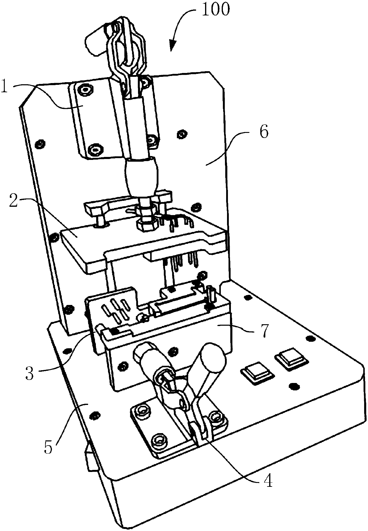
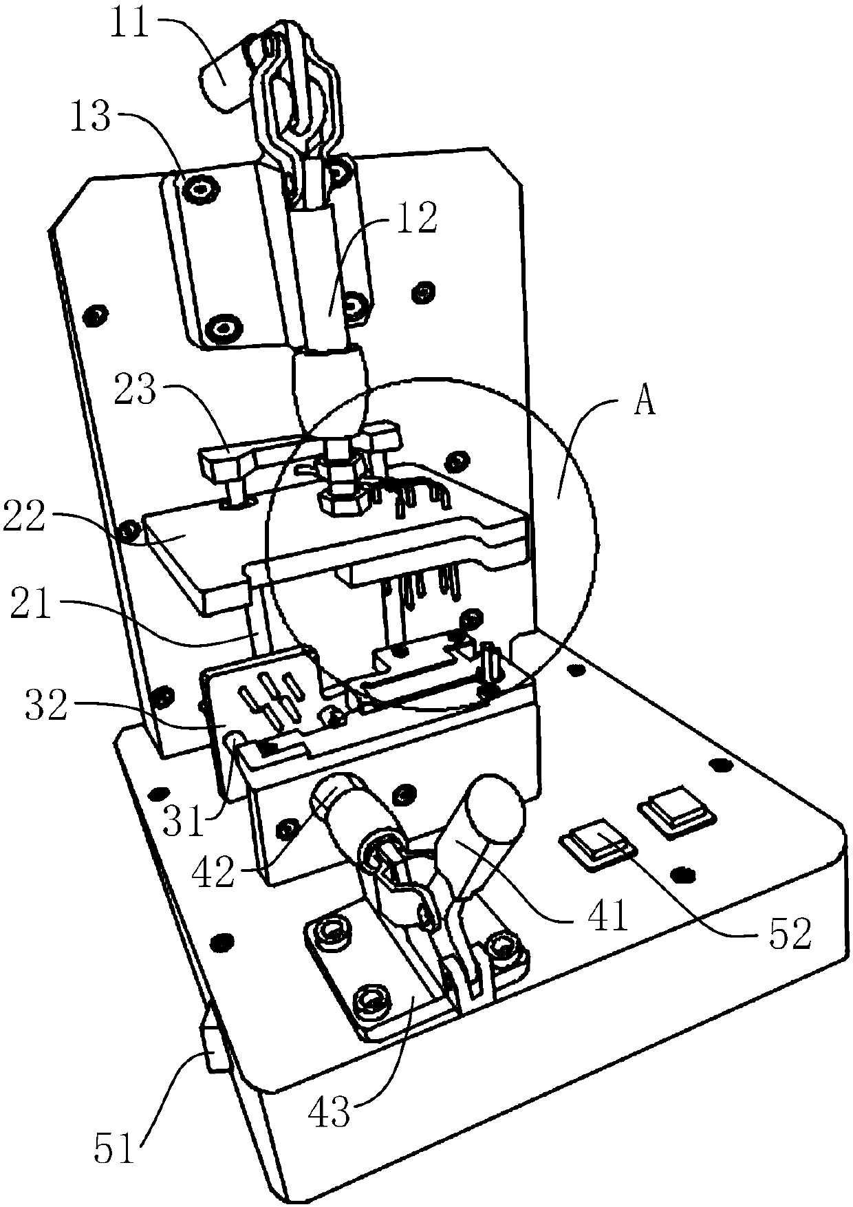
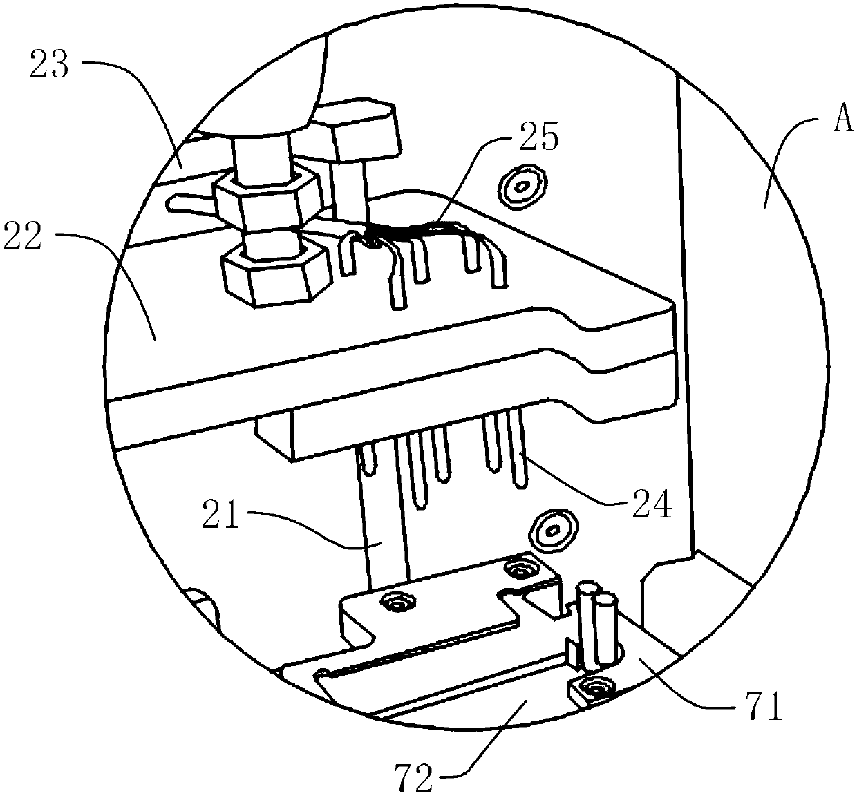
[0027] A double-sided circuit board testing device such as Figure 1-Figure 3 As shown, the test device body 100 is included, and the test device body 100 includes a longitudinal detection mechanism 2, a horizontal detection mechanism 3, a test base 5, a vertical side plate 6, and a feeding mechanism 7; the feeding mechanism 7 is fixedly installed on the test base 5, The vertical side plate 6 is located on one side of the feeding mechanism 7 and is fixedly installed on the test base 5, the longitudinal detection mechanism 2 is connected to the vertical side plate 6 and is located above the feeding mechanism 7, and the horizontal detection mechanism 3 i...


PUM


Abstract

The invention provides a double-sided circuit board testing device. The device includes a testing device body, the testing device body comprises a longitudinal detection mechanism, a transverse detection mechanism, a test base, a vertical side plate, and a feeding mechanism. The feeding mechanism is fixedly installed on the test base, the vertical side plate is located on one side of the feeding mechanism and fixedly installed on the test base, the longitudinal detection mechanism and the vertical side plate are connected and located above the feeding mechanism, and the transverse detection mechanism and the vertical side plate are connected and located between the feeding mechanism and the vertical side plate; the transverse detection mechanism is connected with a lifting mechanism, the transverse detection mechanism is connected with a moving mechanism, and the longitudinal detection mechanism and the transverse detection mechanism are provided with detection probes corresponding totest contacts on a double-sided circuit board. By testing the two sides of the double-sided circuit board at the same time, labor is thus reduced, the working time is reduced, the production efficiency is improved, the cost is reduced, the practicability is high and the device is easy to popularize.

Description

technical field [0001] The invention relates to the field of circuit board testing, in particular to a double-sided circuit board testing device. Background technique [0002] Domestic research on the automatic detection system of printed circuit boards began in the early and mid-1990s, and it has just started. There are relatively few scientific research institutes engaged in research in this area, and because of the influence of various factors, the research on the automatic optical inspection system for printed circuit board defects also stays at a relatively early level. Because the automatic detection system of printed circuit boards in foreign countries is too expensive, and the automatic detection equipment of printed circuit boards in the true sense has not been developed in China, most domestic circuit board manufacturers still use manual inspection with a magnifying glass or a projector. method to check the side. Due to the high labor intensity of manual inspecti...

Claims


Application Information

Patent Timeline
Patent Type & Authority Applications(China)
IPC IPC(8): G01R31/28
CPCG01R31/2806
Inventor 高平韩志颖高二平陈元喜
Owner GUANGDONG FEIKETE ELECTRONICS TECH CO LTD
Why Eureka
Try Eureka