Meta-structure surface member generating nanometer scale vertical light spot chain and generation method thereof
A metasurface, nanoscale technology, applied in optical components, optics, instruments, etc., to achieve the effect of easy integration
- Summary
- Abstract
- Description
- Claims
- Application Information
AI Technical Summary
Problems solved by technology
Method used
Image
Examples
Embodiment Construction
[0025] In order to make the purpose, technical solutions and advantages of the embodiments of the present invention clearer, the technical solutions in the embodiments of the present invention will be clearly and completely described below in conjunction with the drawings in the present invention. Apparently, the described embodiments are some, but not all, embodiments of the present invention.
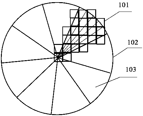
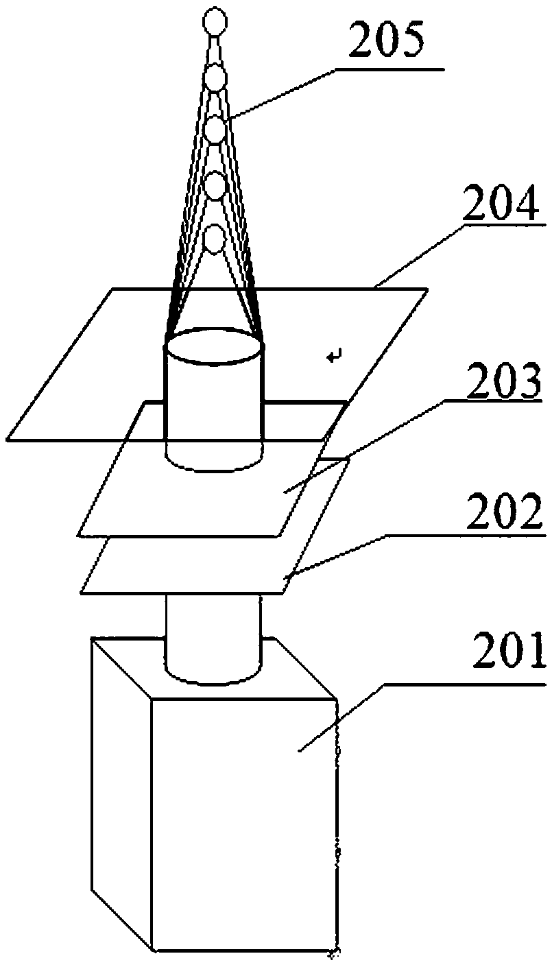
[0026] First determine the size of the metasurface element to be designed, the base material used, the number of spots to be generated and the spacing. In this embodiment, the shape of the metasurface element is square, the side length is 80 microns, and the base material is quartz glass with a thickness of 0.17 mm. The focal plane is 60 microns, and the number of spots is 5. The laser wavelength used is 633 nm. Follow the steps below to design, manufacture and verify:
[0027] Step 1: Coating a film on the base material, and determining the side length of the sub-wavelength square...
PUM
 Abstract
Description
Claims
Application Information


