Display panel and preparing method thereof

A technology for display panels and display areas, which is used in semiconductor/solid-state device manufacturing, organic light-emitting device manufacturing/processing, and semiconductor/solid-state device testing/measurement, etc. Monitoring and other issues to achieve the effect of extending the service life

Active Publication Date: 2018-02-27
BOE TECH GRP CO LTD
View PDF11 Cites 21 Cited by
  • Summary
  • Abstract
  • Description
  • Claims
  • Application Information

AI Technical Summary

Problems solved by technology

[0004] However, after the encapsulation process of the OLED device is completed, it is difficult to monitor whether the thin-film encapsulation layer is damaged and its encapsulation effect, so th

Method used


Image

  • Display panel and preparing method thereof
  • Display panel and preparing method thereof
  • Display panel and preparing method thereof

Examples


Embodiment 1

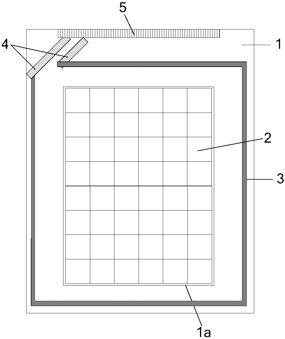
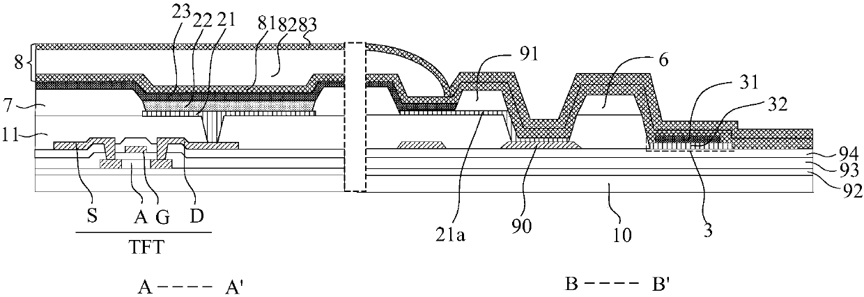
[0034] Such as figure 1 As shown, Embodiment 1 of the present invention provides a display panel, including a substrate 1, and the substrate 1 is divided into a display area 1a; the above-mentioned display panel further includes: a plurality of OLED units 2 arranged in the display area 1a; and setting On the above-mentioned substrate 1 and the monitoring electrode 3 located outside the display area 1a, the resistance value of the monitoring electrode 3 changes after reacting with water and / or oxygen; at least the film encapsulation layer covering the display area 1a and on the monitoring electrode 3 (not shown in the figure).

[0035] It should be noted that, firstly, the aforementioned substrate is specifically an array substrate (Array, or called a backplane) on which an array layer of thin film transistors is formed.

[0036] Second, the pattern of the above-mentioned monitoring electrode 3 is not limited to figure 1 A ring with an opening shown in , as long as it is plac...

Embodiment 2

[0083] An embodiment of the present invention also provides a method for preparing the above-mentioned display panel. The preparation method includes: the steps of forming a plurality of OLED units in the display area of ​​the substrate and forming monitoring electrodes outside the display area; Or the resistance value changes after the oxygen reacts; the step of forming a thin film encapsulation layer covering at least the display area and the monitoring electrodes.

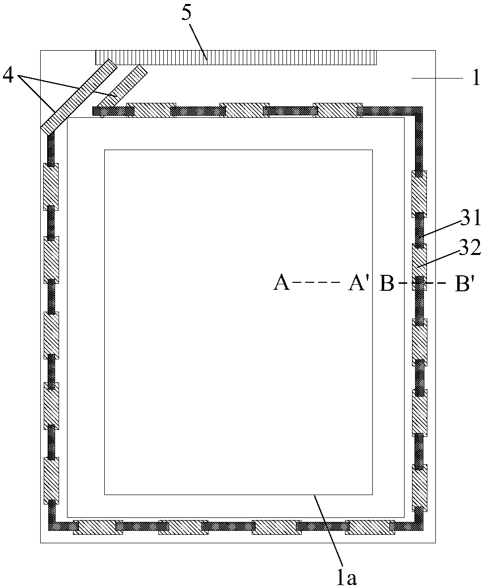
[0084] Further, in order to improve the monitoring efficiency, the formed monitoring electrode is specifically a monitoring ring surrounding the display area; the monitoring ring is provided with openings; the above preparation method also includes: the step of forming test leads respectively connected to the two ends of the opening on the substrate .

[0085] Further, the step of forming the monitoring ring includes: forming a plurality of spaced connection electrodes around the display area of ​​the substrate;...


PUM


Abstract

The invention provides a display panel and a preparing method thereof, and relates to the technical field of displaying. Whether encapsulation of the display panel is invalid or not can be monitored through change of the resistance value of a monitoring electrode located outside a display area to further monitor the water-and-oxygen corrosion degree and the service life of OLED units at the edge of the display area in the display panel. The display panel comprises a substrate, and the substrate is divided into the display area; the display panel further comprises multiple OLED units, the monitoring electrode and a thin film encapsulation layer, wherein the multiple OLED units are arranged in the display area, the monitoring electrode is arranged on the substrate and is located outside thedisplay area, and the resistance value is changed after the monitoring electrode reacts with water and/or oxygen; the thin film encapsulation layer at least covers the inside of the display area and the monitoring electrode.

Description

technical field [0001] The invention relates to the field of display technology, in particular to a display panel and a preparation method thereof. Background technique [0002] Organic Light-Emitting Display (OLED) is rapidly emerging in the field of display due to its advantages of ultra-thin, low power consumption, high brightness, high luminous efficiency and being applicable to flexible displays, but its service life Shorter defects have been restricting its development. The erosion of OLED devices by water and oxygen is the main reason affecting their service life. On the one hand, the cathodes of OLED devices are usually metals with relatively active chemical properties, which are prone to electrochemical corrosion in a water-oxygen environment and cause device failure; on the other hand, oxygen is prone to oxidation with the light-emitting functional layer in OLED devices. The generated carbonyl compound is an effective quencher, which will reduce the luminous quan...

Claims


Application Information

Patent Timeline
IPC IPC(8): H01L27/32H01L51/52H01L21/66
CPCH01L22/14H01L22/34H10K59/12H10K50/805H10K50/30Y02E10/549H10K59/1213H10K59/131H10K71/70H10K50/844H10K2102/00H10K71/00H10K50/841H10K50/81H10K50/82H10K59/122H10K77/10
Inventor 王伟
Owner BOE TECH GRP CO LTD
Why Eureka
Try Eureka