

Fin line type orthogonal-mode coupler based on double-ridge step structure
A technology of orthogonal mode coupler and steps, which is applied in the direction of waveguide devices, electrical components, connecting devices, etc., can solve the problem that the in-band return loss characteristics of fin-line OMTs can not be fully considered relative to the working bandwidth, and achieve reduction Effects of device insertion loss, overall compactness, and wide bandwidth
- Summary
- Abstract
- Description
- Claims
- Application Information
AI Technical Summary
Problems solved by technology
Method used
Image

Examples
Embodiment 1
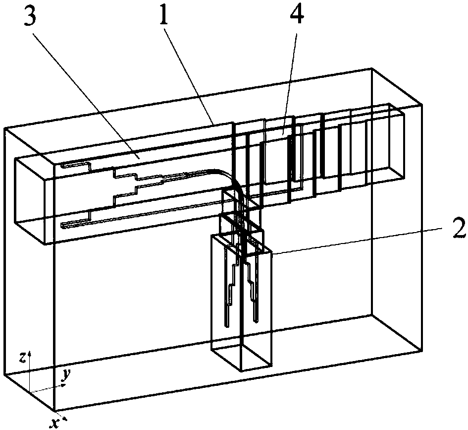
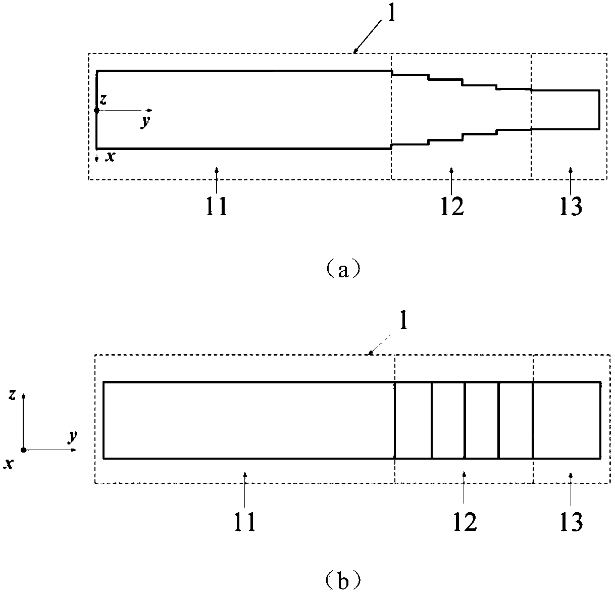
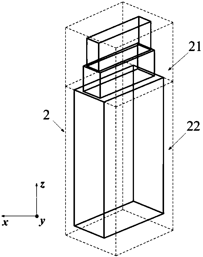
[0033] refer to figure 1 , a fin linear orthogonal mode coupler based on a double ridge step structure, including a waveguide body, the waveguide body adopts a three-port T-shaped waveguide structure composed of a horizontal waveguide 1 and a vertical waveguide 2 perpendicular to each other, wherein the horizontal waveguide 1 Sectional diagram of xoy plane figure 2 As shown in (a), the cross-sectional view of the xoz plane of the horizontal waveguide 1 is as follows figure 2 As shown in (b), the structural schematic diagram of the vertical waveguide 2 is as follows image 3 As shown, the T-shaped waveguide structure is symmetrical about the yoz plane, and a metal ridge 3 and an impedance absorbing piece 4 with a thickness of 0.4mm are installed next to the yoz symmetry plane of the waveguide structure, and the metal ridge 3 It consists of two parts, the horizontal metal ridge 31 and the vertical metal ridge 32, wherein the yoz section diagram of the horizontal metal ridge ...
Embodiment 2
[0040] Embodiment 2, the structure of this embodiment is the same as that of Embodiment 1, only for the resistance value R per square centimeter of the impedance absorbing sheet and the number of stepped gaps N on the horizontal metal ridge sheet 31 1 And each step parameter and the step-like gap series number N on the vertical metal ridge sheet 32 2 And the parameters of each step are adjusted:
[0041] Impedance absorbing sheet 4 adopts the ITO conductive glass material whose impedance value per square centimeter is R=50Ω; in the horizontal metal ridge sheet 31, the number of steps on the gap is 3, and each step is mirror-symmetrical about the longitudinal central axis of the metal patch, and the steps The length and spacing along the negative direction of the y-axis are 2.56mm×4.5mm, 2.26mm×2mm, 2.02mm×0.5mm respectively; in the vertical metal ridge 32, the number of steps on the gap is 2, and each step is about The longitudinal central axis of the sheet is mirror-symmetri...
Embodiment 3
[0042] Embodiment 3, the structure of this embodiment is the same as that of Embodiment 1, only for the resistance value R per square centimeter of the impedance absorbing sheet and the number of stepped gaps N on the horizontal metal ridge sheet 31 1 And each step parameter and the step-like gap series number N on the vertical metal ridge sheet 32 2 And the parameters of each step are adjusted:
[0043] Impedance absorbing sheet 4 adopts the ITO conductive glass material whose impedance value per square centimeter is R=500Ω; in the horizontal metal ridge sheet 31, the number of steps on the gap is 9, and each step is mirror-symmetrical about the longitudinal central axis of the metal patch, and the steps The length and spacing along the negative direction of the y-axis are 2.56mm×5mm, 2.26mm×4.2mm, 2.02mm×3.5mm, 2.02mm×2.75mm, 2.02mm×2.1mm, 2.02mm×1.5mm, 2.02mm× 1mm, 2.02mm×0.6mm, 2.02mm×0.25mm; in the vertical metal ridge 32, the number of steps on the gap is 8, each step i...
PUM
 Abstract
Description
Claims
Application Information