Multi-wavelength tunable surface plasmon resonance imaging device and its application

A surface plasmon and resonance imaging technology, used in measurement devices, instruments, scientific instruments, etc., can solve the problems of SPR image distortion and limitations, and achieve the effect of improving dynamic range and improving detection performance.

Active Publication Date: 2020-05-05
NANJING UNIV
View PDF10 Cites 0 Cited by
  • Summary
  • Abstract
  • Description
  • Claims
  • Application Information

AI Technical Summary

Problems solved by technology

In the angle modulation mode, as the incident angle changes, the SPR image on the chip will be distorted; in the wavelength modulation mode, the resonance spectral distribution is obtained by scanning the wavelength of the incident light or using a spectrometer as a detector ; The former measurement mode can perform synchronous scanning detection on 2-dimensional arrays, and has 2-dimensional imaging capabilities, while the latter provides instantaneous spectral information, but can only be limited to 1-dimensional array scanning
Therefore, combining wavelength-modulated and high-throughput data acquisition with SPRI technology remains a challenge

Method used


Image

  • Multi-wavelength tunable surface plasmon resonance imaging device and its application
  • Multi-wavelength tunable surface plasmon resonance imaging device and its application
  • Multi-wavelength tunable surface plasmon resonance imaging device and its application

Examples


Embodiment Construction

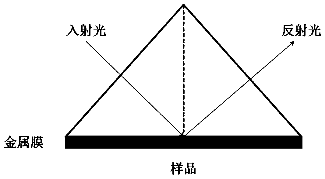
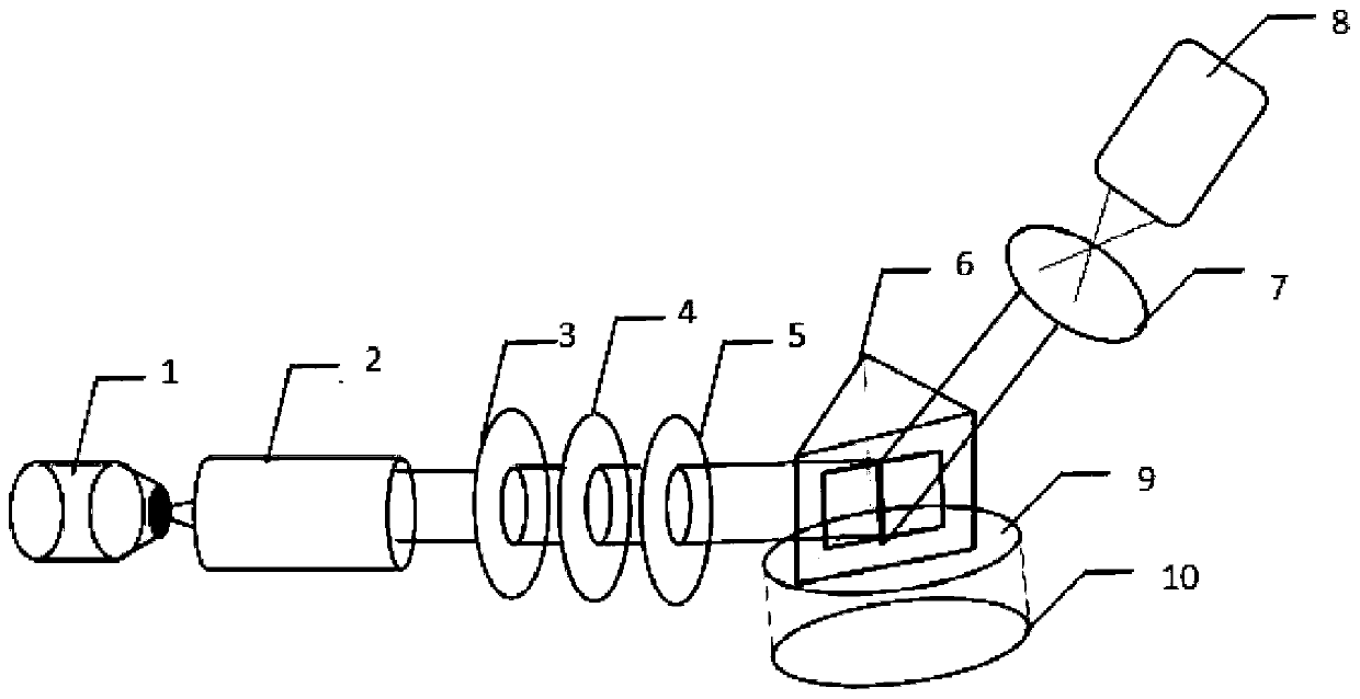
[0021] On the basis of the traditional single-wavelength filter SPRI imaging optical path, the present invention designs a multi-band broadband LED light source (Light source), linear variable bandpass filter (Linear Variable Bandpass Filters), collimating mirror (Collimator lens), motorized stage (Motorized Stages), objective lens (Objective) and CCD camera combination system, mainly using linear variable bandpass filter and motorized stage in the existing SPRI imaging device . Its structure is as image 3 shown.

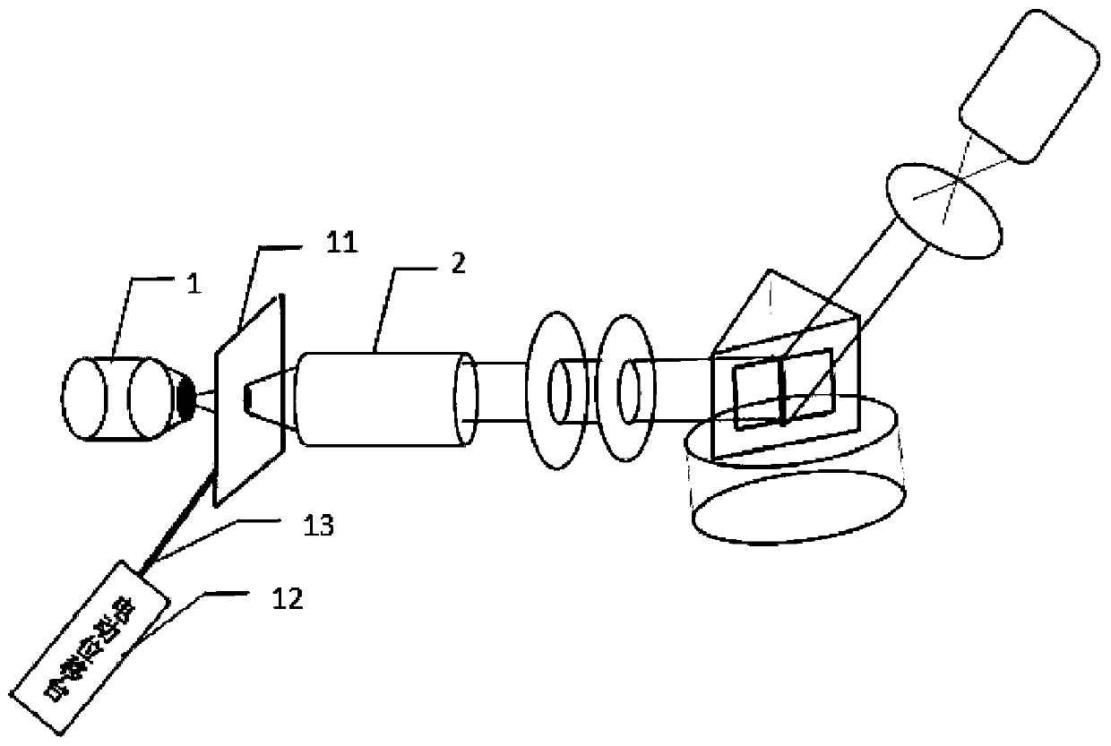
[0022] Figure 1~4 Among them, 1 is the light source, 2 is the collimating mirror, 3 is the aperture, 4 is the polarizer, 5 is the filter, 6 is the prism, 7 is the lens, 8 is the camera, 9 is the longitudinal adjustment platform, and 10 is the angle adjustment platform , 11 is a linear bandpass filter, 12 is an electric shift table, and 13 is a connecting rod.

[0023] By adding a filter device linear variable bandpass filter 11 between the light source 1 and t...


PUM


Abstract

The invention discloses a multi-wavelength adjustable surface plasma resonance imaging device and application thereof. Light beams transmitted by an LED light source with a broad-band spectrum are filtered by using a linear light filter to obtain monochromatic light beams; then the monochromatic light beams from a polarization light source, which projects to an SPR (Surface Plasmon Resonance) generation device, through a collimating mirror and a polarizer. Outgoing light beams of the device are imaged by a CCD (Charge Coupled Device) camera; a mobile platform also can be used for controlling the linear light filter to linearly adjust the wavelength of the light source, and multiband incident light can be obtained for SPR imaging; all areas of the surface of the chip can be subjected to waveband scanning at the same time to obtain resonance spectra of all the areas; and under the condition of ensuring that SPRI (Surface Plasmon Resonance Imaging) has no distorsion, resonance spectrum offsets generated by environment change of all the areas on the surface of a sensing chip are accurately measured. By using the method, data of all the areas on the surface of the chip can reach optimumsensitivity conditions, dynamic range of instrument detection is widened, and the sensitivity of the instrument detection is improved.

Description

technical field [0001] The invention belongs to the field of instruments and equipment, and in particular relates to a Kretschmann type SPR imaging device and method. Background technique [0002] The surface plasmon resonance (Surface Plasmon Resonance, SPR) phenomenon is a physical phenomenon, which refers to the physical optical process in which the free vibration electrons existing on the metal surface are excited by light under certain conditions, and the ability to absorb light resonates. [0003] When light is projected from an optically denser medium to an optically rarer medium, when the incident angle is greater than a certain angle (critical angle), total reflection occurs. The incident light and the medium surface normal constitute the incident plane, and the electric field of the incident light wave can be decomposed into two mutually orthogonal polarized light components, one is the transverse magnetic wave in the incident plane, which is called TM wave or p-po...

Claims


Application Information

Patent Timeline
Patent Type & Authority Patents(China)
IPC IPC(8): G01N21/552
CPCG01N21/553
Inventor 许丹科贾文超李慧
Owner NANJING UNIV
Why Eureka
Try Eureka