

Semiconductor device and manufacturing method thereof
A semiconductor and buffer layer technology, applied in the field of semiconductor devices and their manufacturing, can solve problems such as reducing the full well electron capacity of an image sensor, and achieve the effects of improving image quality, improving quantum efficiency, and reducing crosstalk
- Summary
- Abstract
- Description
- Claims
- Application Information
AI Technical Summary
Problems solved by technology
Method used
Image

Examples
Embodiment Construction
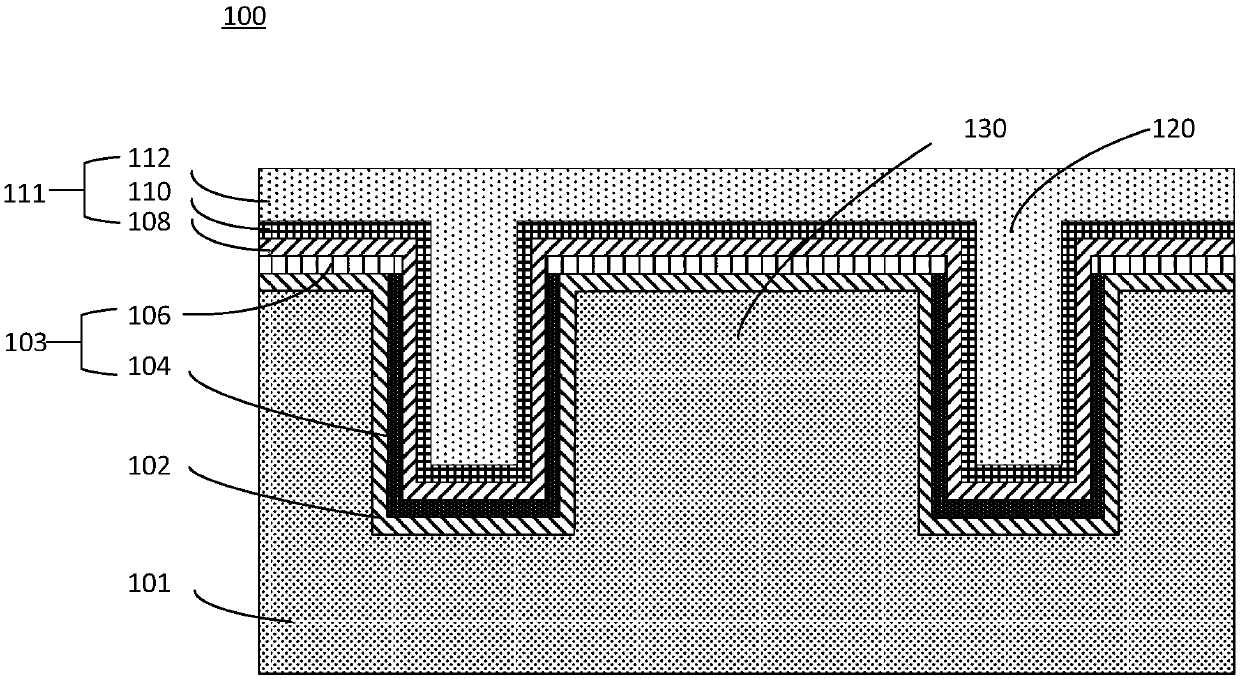
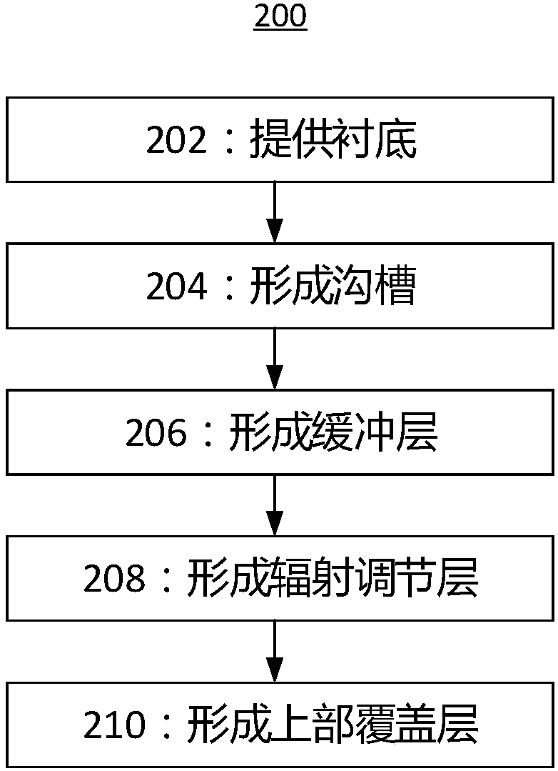
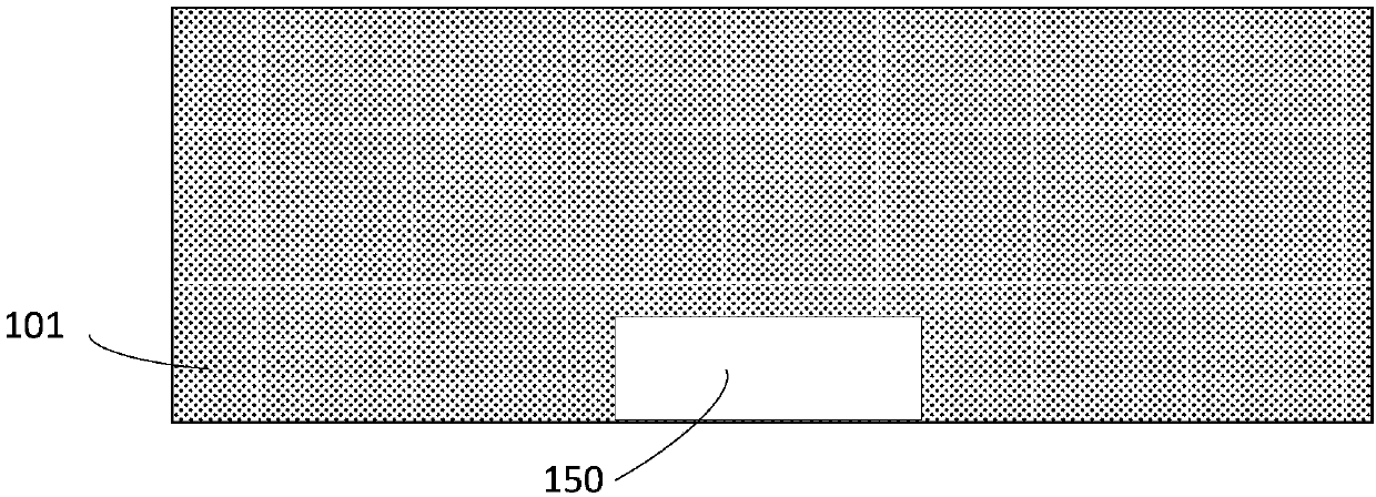
[0045]Various exemplary embodiments of the present disclosure will now be described in detail with reference to the accompanying drawings. It should be noted that the relative arrangements of components and steps, numerical expressions and numerical values set forth in these embodiments do not limit the scope of the present disclosure unless specifically stated otherwise. In addition, techniques, methods, and devices known to persons of ordinary skill in the related art may not be discussed in detail, but where appropriate, such techniques, methods, and devices should be considered part of the authorized specification.
[0046] In the specification and claims, the words "front", "rear", "top", "bottom", "above", "under", etc., if present, are used for descriptive purposes and not necessarily to describe a constant relative position. It is to be understood that the terms so used are interchangeable under appropriate circumstances such that the embodiments of the disclosure d...
PUM
 Abstract
Description
Claims
Application Information