Superjunction device and method of manufacturing the same

A super-junction device, N-type technology, applied in semiconductor/solid-state device manufacturing, semiconductor devices, electrical components, etc., can solve the problem of not being able to improve the reverse recovery softness factor of the body diode of the device

Active Publication Date: 2020-12-08
SHENZHEN SANRISE TECH CO LTD
View PDF4 Cites 0 Cited by
  • Summary
  • Abstract
  • Description
  • Claims
  • Application Information

AI Technical Summary

Problems solved by technology

However, in the existing structure, the carriers in the N-P column are completely exhausted when Vds is less than 50V, so even if the operating voltage Vdd is as small as 200V V to 300V, the remaining carriers after the device voltage reaches Vdd are only N-P part of the carriers in the part of the N-type buffer layer 30 under the pillars, so that the softness factor of the device body diode in reverse recovery cannot be improved

Method used


Image

  • Superjunction device and method of manufacturing the same
  • Superjunction device and method of manufacturing the same
  • Superjunction device and method of manufacturing the same

Examples


Embodiment 1

[0083] Embodiment 1 of the present invention super junction device:

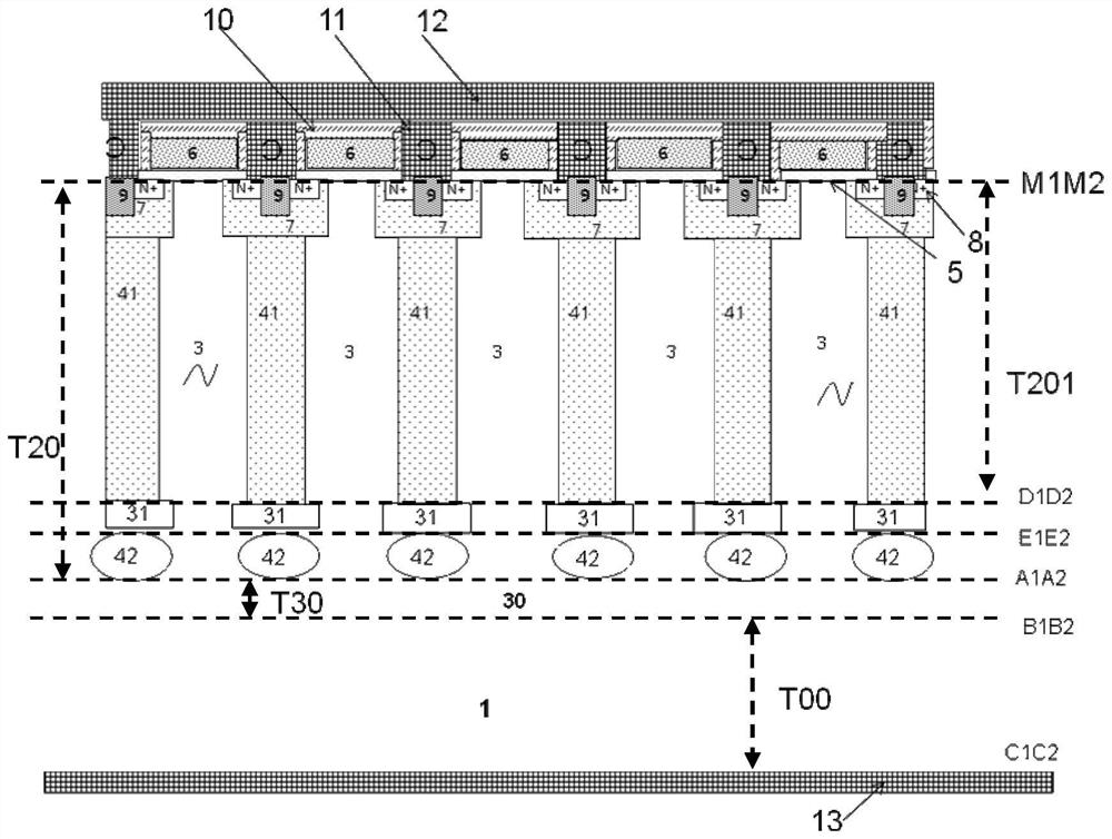
[0084] Such as image 3 Shown is a schematic diagram of a super junction device in Embodiment 1 of the present invention; in Embodiment 1 of the present invention:

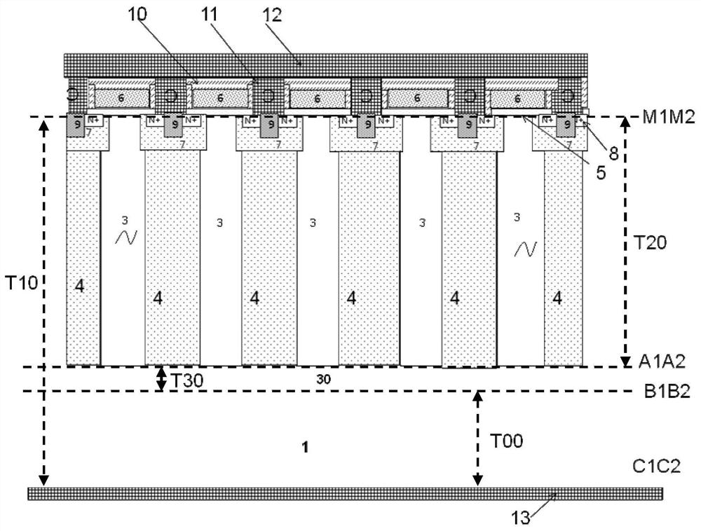
[0085] The charge flow region includes a super junction structure composed of a plurality of alternately arranged N-type pillars 3 and P-type pillars; each of the N-type pillars 3 and its adjacent P-type pillars form a super-junction unit.

[0086] The super junction structure is formed on an N-type epitaxial layer, and an N-type buffer layer 30 composed of an N-type epitaxial layer is formed at the bottom of the super-junction structure, and the bottom of the N-type buffer layer 30 is heavily doped N-type semiconductor substrate 1.

[0087] There is an N-type electric field blocking layer 31 in the P-type column of at least one super junction unit, image 3 It is shown in that all the P-type pillars include an N-type electric field blocking ...


PUM

PropertyMeasurementUnit
thicknessaaaaaaaaaa
thicknessaaaaaaaaaa
electrical resistivityaaaaaaaaaa

Abstract

The present invention discloses a super junction device. P-type columns of at least one super junction unit are internally provided with N-type electric field barrier layers, and the N-type electric field barrier layers are configured to segment the P-type columns into first and second P-type columns which are respectively located at the top portions and the bottom portions of the electric field barrier layers; the N-type electric field barrier layers are configured to realize segmentation exhaustion of super junction structures at a top portion and a bottom portion; when a source-drain voltage of a super junction device is smaller than or equal to a first voltage value, the super junction structure at the top portion is only exhausted; and when the source-drain voltage of the super junction device is larger than the first voltage value, the super junction structures at the top portion and the bottom portion are exhausted. The present invention further discloses a manufacturing methodof a super junction device. According to the invention, a gate-drain capacitance and the minimum value of the gate-drain capacitance can be improved to effectively reduce the electromagnetic interference performance of the device in an application circuit and effectively reduce current and voltage overshoot caused by the device in the application circuit, reversely recovered soft factors of the device can be increased, and a breakdown voltage of the device can be maintained.

Description

technical field [0001] The invention relates to the field of manufacturing semiconductor integrated circuits, in particular to a super junction device; the invention also relates to a method for manufacturing the super junction device. Background technique [0002] The super junction structure is composed of alternately arranged N-type pillars and P-type pillars. If the superjunction structure is used to replace the N-type drift region in the vertical double-diffused MOS transistor (Vertical Double-diffused Metal-Oxide-Semiconductor, VDMOS) device, the conduction path is provided through the N-type column in the conduction state, and when the conduction The P-type column does not provide a conduction path; in the off state, the PN column jointly bears the reverse bias voltage, forming a super-junction metal-oxide-semiconductor field-effect transistor (Metal-Oxide-Semiconductor Field-Effect Transistor, MOSFET). The super-junction MOSFET can greatly reduce the on-resistance o...

Claims


Application Information

Patent Timeline
Patent Type & Authority Patents(China)
IPC IPC(8): H01L29/78H01L21/336H01L29/06
CPCH01L29/0634H01L29/66712H01L29/7802
Inventor 肖胜安曾大杰
Owner SHENZHEN SANRISE TECH CO LTD
Why Eureka
Try Eureka