Electrical atomic force microscope probe adopting conductive nanowires

An atomic force microscope and conductive nanotechnology, applied in scanning probe technology, scanning probe microscopy, measuring devices, etc., can solve problems such as short life, low lateral resolution, and easy wear, so as to improve service life and improve consistent effect

Inactive Publication Date: 2018-03-09
苏州泰岩新材料有限公司
View PDF0 Cites 6 Cited by
  • Summary
  • Abstract
  • Description
  • Claims
  • Application Information

AI Technical Summary

Problems solved by technology

Therefore, the current electrical and conductive probes have low lateral resolution, and are prone to wear and have a short life.

Method used


Image

  • Electrical atomic force microscope probe adopting conductive nanowires

Examples


Embodiment Construction

[0016] The following will clearly and completely describe the technical solutions in the embodiments of the present invention with reference to the accompanying drawings in the embodiments of the present invention. Obviously, the described embodiments are only some of the embodiments of the present invention, not all of them. All other embodiments obtained by persons of ordinary skill in the art based on the embodiments of the present invention belong to the protection scope of the present invention.

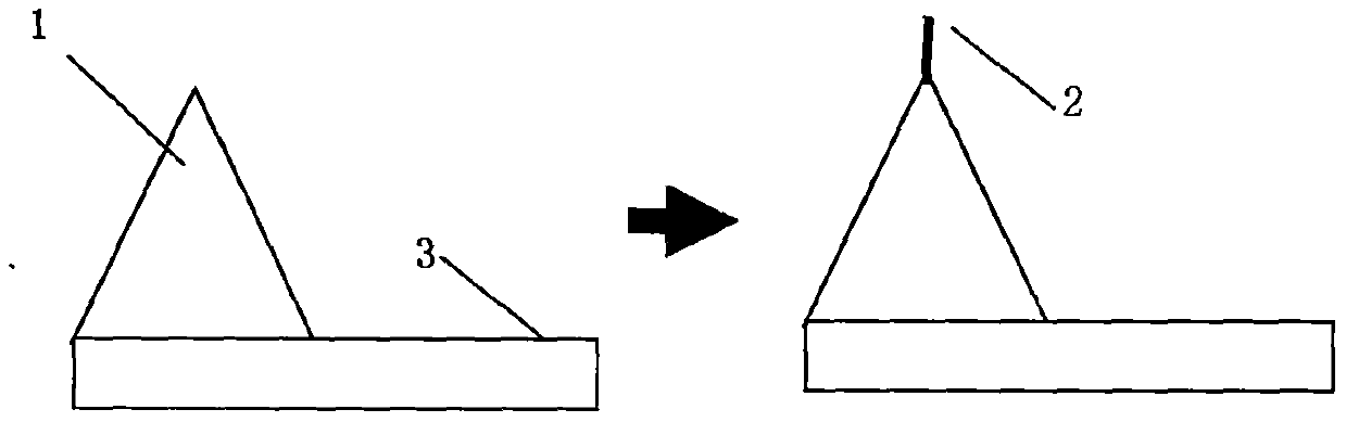
[0017] The invention adopts the conventional atomic force microscope probe as the basis, and utilizes the advantages of the probe being easy to obtain, cheap, diverse and optional, and stable. At the same time, the advantages of large aspect ratio and ultra-high resolution of conductive nanowires are used to prepare electrical and conductive AFM probes with excellent performance.

[0018] Such as figure 1 As shown, the electrical and conductive atomic force microscope probe acc...


PUM

PropertyMeasurementUnit
lengthaaaaaaaaaa
diameteraaaaaaaaaa
thicknessaaaaaaaaaa

Abstract

The invention discloses an electrical and conductive atomic force microscope probe using conductive nanowires and a preparation method thereof, which solves the bottleneck problem of the current electrical and conductive atomic force microscope probe, and greatly improves the service life and resolution of the atomic force microscope probe. The conductive nanowire probe can be prepared by direct bonding method and chemical vapor deposition growth method. Fully utilizing the ultra-high resolution and ultra-long service life of the conductive one-dimensional nanomaterial probe, it solves the long-term problems of short life and easy wear of the electrical and conductive atomic force microscope probes, improves the consistency of the test, and meets It meets the needs of different application fields such as scientific research, production and teaching.

Description

【Technical field】 [0001] The invention relates to the field of atomic force microscopy, in particular to a long-life high-resolution electrical and conductive atomic force microscopy probe and a preparation method thereof. 【Background technique】 [0002] Atomic Force Microscope (AFM, Atomic Force Microscope) is an important instrument with atomic-level resolution for the analysis of surface morphology, heat, force, electricity, magnetism, optics and other properties. An important characterization tool in the life sciences and more. An atomic force microscope scans the surface of a sample with a very sharp tip attached to a cantilever. The force deflection of the cantilever is detected by the position change of the reflected light of the laser beam, and then processed by a computer to generate a surface topography image. Among them, the AFM probe is the key sensor in the atomic force microscope. As a daily consumable, its main manufacturers are distributed in Germany, Swit...

Claims


Application Information

Patent Timeline
Patent Type & Authority Applications(China)
IPC IPC(8): G01Q60/40
CPCG01Q60/40
Inventor 不公告发明人
Owner 苏州泰岩新材料有限公司
Why Eureka
Try Eureka