Eureka AIR delivers breakthrough ideas for toughest innovation challenges, trusted by R&D personnel around the world.

Embedded-type touch control panel and preparation method thereof

A touch panel and embedded technology, applied in the field of embedded touch panel and its preparation, can solve the problems of mutual interference, weak anti-signal interference, low yield and the like, so as to prevent mutual signal interference and improve touch sensitivity. , the effect of simplification of processing technology

Inactive Publication Date: 2018-03-13
WGTECH JIANGXI
View PDF4 Cites 4 Cited by
  • Summary
  • Abstract
  • Description
  • Claims
  • Application Information

AI Technical Summary

Problems solved by technology

In the traditional embedded touch panel, the first electrode is set on the PEP film or glass, and the second electrode is set on the PEP film or glass, and then the first electrode and the second electrode are connected with the color filter embedded in the display screen. Between the optical sheet substrate and the polarizer, however, the touch panel with this structure is relatively thick, which cannot meet the needs of light and thin
[0003] In order to reduce the thickness, one method is to arrange the first electrode and the second electrode on the same electrode layer, however, the processing technology of arranging the first electrode and the second electrode on the same electrode layer is complicated, the yield rate is low, and the first The electrode and the second electrode are relatively close to each other, which is prone to mutual interference
Since the human body itself is a conductor, in practical applications, when a finger touches the touch panel, it may affect the power line and change the capacitance without applying force.
Especially when the finger has strong static electricity, oil stains or the touch screen is in contact with a charged object, there will be signal interference, which will affect the precise position of finger touch recognition
[0004] To sum up, the traditional embedded touch panel is thick and has weak anti-signal interference ability

Method used


Image

  • Embedded-type touch control panel and preparation method thereof
  • Embedded-type touch control panel and preparation method thereof
  • Embedded-type touch control panel and preparation method thereof

Examples


preparation example Construction

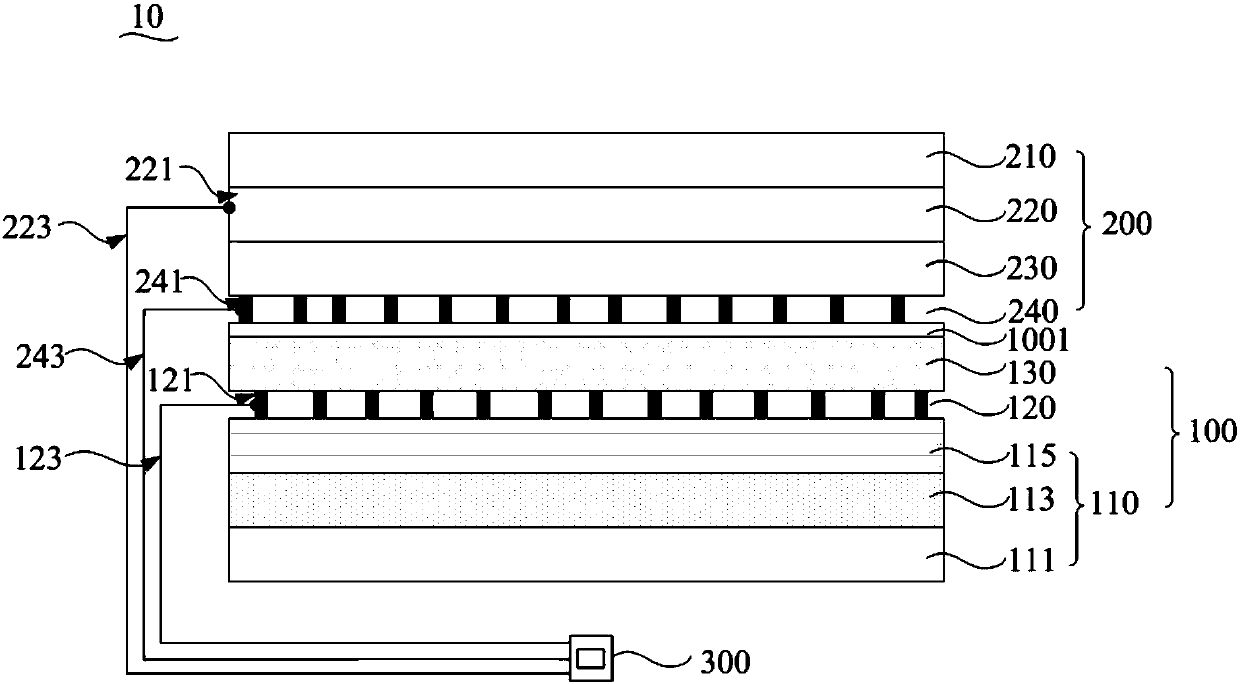
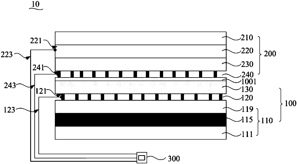
[0070] The method for manufacturing the above-mentioned embedded touch panel 10 according to one embodiment includes the following steps S110-S170.

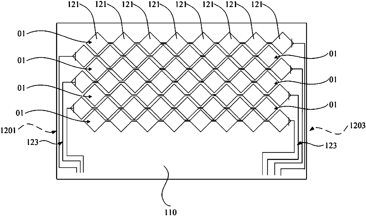
[0071] S110, forming a first electrode on the TFT display panel, the first electrode includes a plurality of first electrode blocks arranged in an array and first electrode leads electrically connected to the first electrode blocks.

[0072] Specifically, a layer of transparent conductive film can be obtained on the TFT display panel by magnetron sputtering or glue coating, and the thickness of the film is 900nm-1000nm. The raw material of the conductive film layer can be ITO, AZO or graphene. Graphene material is preferred if used for flexible panels. The first electrode block is formed by sequentially applying glue, photolithography, developing, etching, and peeling off the glue. Then the first electrode leads are formed by metal etching.

[0073] S120 , covering the first electrode with a polarizer to obtain a sensing compo...

Embodiment 1

[0090] A TFT display panel is provided, and the TFT display panel includes a TFT substrate, a liquid crystal layer and a color filter stacked in sequence.

[0091] A layer of ITO transparent conductive film layer is formed on the color filter by magnetron sputtering method, and the thickness of the film layer is 950nm. On the transparent conductive film layer, a first electrode block is formed sequentially through glue coating, photolithography, development, etching, and glue stripping, and then a first electrode lead is formed through metal etching to obtain a first electrode. For the design of the first electrode see figure 2 shown. The surface resistance of the prepared first electrode was 33Ω, and the transmittance was 97%. A polarizer is covered on the first electrode to obtain a sensing component. Wherein the polarizer covers the surface of each first electrode block, and the polarizer covers the area of ​​the surface of the TFT display panel not covered by the first...

Embodiment 2

[0099] (1) Preparation of induction components

[0100] A TFT display panel is provided, and the TFT display panel includes a TFT substrate, a liquid crystal layer and a color filter stacked in sequence.

[0101] A layer of AZO transparent conductive film is formed on the color filter by magnetron sputtering method, and the film thickness is 900nm. On the transparent conductive film layer, a first electrode block is formed sequentially through glue coating, photolithography, development, etching, and glue stripping, and then a first electrode lead is formed through metal etching to obtain a first electrode. For the design of the first electrode see figure 2 shown. The surface resistance of the prepared first electrode was 30Ω, and the transmittance was 98%. A polarizer is covered on the first electrode to obtain a sensing component. Wherein the polarizer covers the surface of each first electrode block, and the polarizer covers the area of ​​the surface of the TFT display...


PUM

PropertyMeasurementUnit
Thicknessaaaaaaaaaa
Thicknessaaaaaaaaaa
Surface resistanceaaaaaaaaaa

Abstract

The invention relates to an embedded-type touch control panel and a preparation method thereof. The embedded-type touch control panel includes a sensing component, a triggering component and an electrode interface. A first electrode is arranged on a TFT display panel, a second electrode is arranged on a silicon dioxide layer, and the surface, away from the silicon dioxide layer, of the second electrode is fitted on a polaroid to make the sensing component combined with the triggering component. The designed embedded-type touch control panel has the advantages of being lightweight, thin and high in noise resistance.

Description

technical field [0001] The invention relates to the field of display devices, in particular to an embedded touch panel and a preparation method thereof. Background technique [0002] Touch screens are an important part of electronic devices such as mobile phones, tablet computers, and e-books. Capacitive touch screen technology uses the current induction of the human body to work. When a finger touches the touch screen, the capacitance of the contact will change, causing the frequency of the oscillator connected to it to change. By measuring the frequency change, the touch position can be determined to obtain information. Embedded touch panel (on-cell touch panel) refers to the method of embedding the touch panel between the color filter substrate and the polarizer of the display screen, that is, a touch sensor is equipped on the liquid crystal panel. In the traditional embedded touch panel, the first electrode is set on the PEP film or glass, and the second electrode is s...

Claims


Application Information

Patent Timeline
IPC IPC(8): G02F1/1343G02F1/1335G02F1/1333G02F1/1345G06F3/041
CPCG02F1/133345G02F1/13338G02F1/133528G02F1/134309G02F1/1345G02F2202/22G06F3/041
Inventor 易伟华张迅张伯伦周慧蓉
Owner WGTECH JIANGXI
Why Eureka
Eureka Blog
Learn More