Method for forming semiconductor structure

A semiconductor and transistor technology, applied in the field of semiconductor structure formation, can solve the problem that the performance of the semiconductor structure needs to be improved, and achieve the effects of strong protection ability, reducing damage and improving performance

Active Publication Date: 2018-03-13
SEMICON MFG INT (SHANGHAI) CORP +1
View PDF6 Cites 0 Cited by
  • Summary
  • Abstract
  • Description
  • Claims
  • Application Information

AI Technical Summary

Problems solved by technology

[0004] However, even with the introduction of a work function layer in the high-K metal gate stru

Method used


Image

  • Method for forming semiconductor structure
  • Method for forming semiconductor structure
  • Method for forming semiconductor structure

Examples


Embodiment Construction

[0012] It can be seen from the background art that the semiconductor structure introducing the work function layer in the prior art has the problem of poor performance. Now combine the formation method of a semiconductor structure to analyze the reasons for its poor performance:

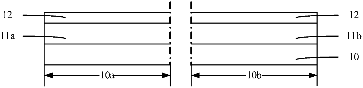
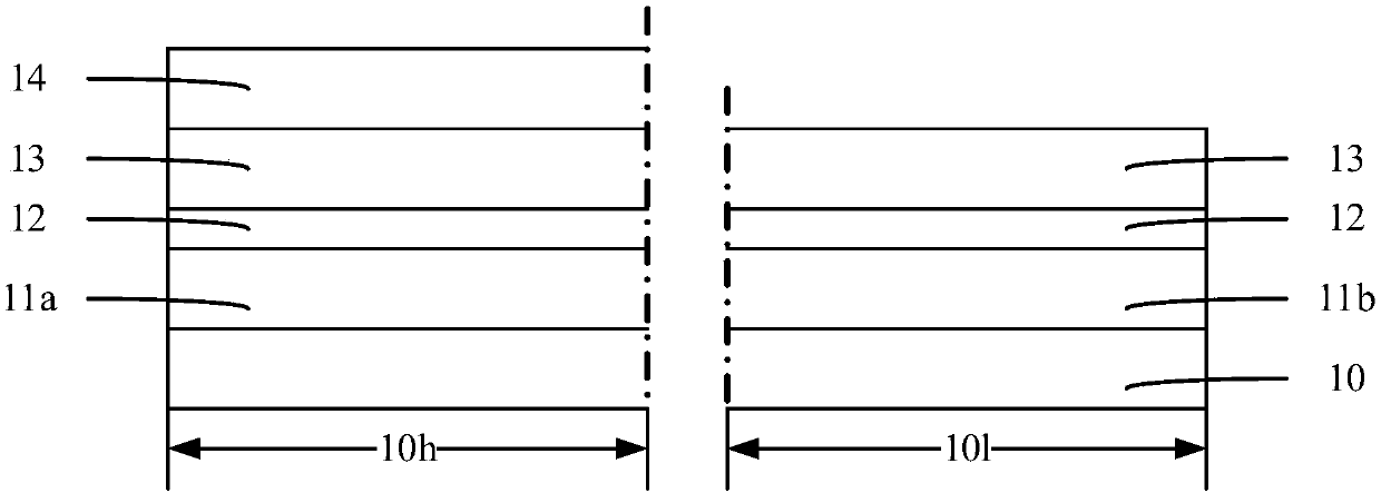
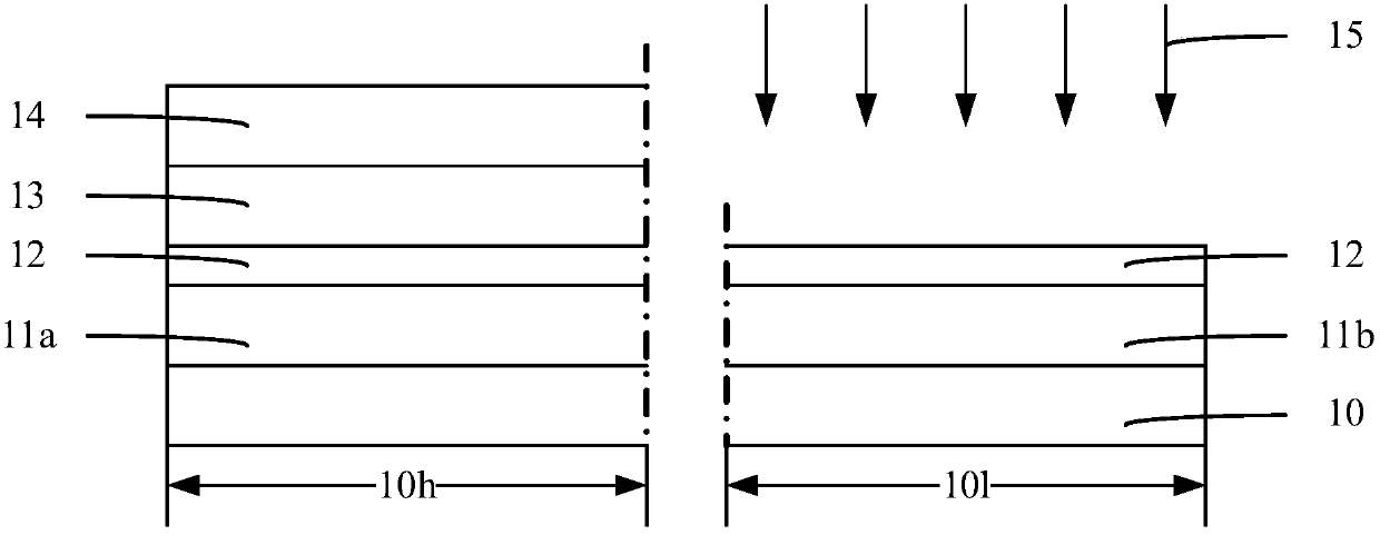
[0013] refer to Figure 1 to Figure 5 , shows a schematic cross-sectional structure corresponding to each step of a method for forming a semiconductor structure.

[0014] refer to figure 1 , providing a substrate 10, the substrate 10 includes a first region 10a and a second region 10b for forming an N-type transistor, the threshold voltage of the transistor in the first region is higher than the threshold voltage of the transistor in the second region 10b.

[0015] continue to refer figure 1 , forming a gate dielectric layer on the substrate 10, the gate dielectric layer on the substrate 10 in the first region 10a is the first gate dielectric layer 11a, and the gate dielectric layer on the substr...


PUM


Abstract

A method for forming a semiconductor structure includes the following steps: forming a substrate which includes a first region and a second region; forming a dummy gate structure; forming an opening;forming a first gate dielectric layer and a second gate dielectric layer; forming a sacrificial layer; forming a first material layer; forming a first mask; exposing the second gate dielectric layer;exposing the first material layer; and forming a second material layer. Compared with the prior art in which the second gate dielectric layer is protected only by the first material layer, in the technical scheme of the invention, the first material layer and the sacrificial layer can better protect the second gate dielectric layer because of larger total thickness, the damage to the second gate dielectric layer in the forming process of the first mask can be effectively reduced, the performance of the gate dielectric layer can be improved, and the performance of a semiconductor structure formed can be improved.

Description

technical field [0001] The invention relates to the field of semiconductor manufacturing, in particular to a method for forming a semiconductor structure. Background technique [0002] With the rapid development of semiconductor manufacturing technology, semiconductor devices are developing towards higher element density and higher integration. As the most basic semiconductor device, transistors are currently being widely used. Therefore, with the improvement of component density and integration of semiconductor devices, the feature size of transistors is getting smaller and smaller. In order to reduce the parasitic capacitance of transistor gates and improve device speed, high The gate structure of the K gate dielectric layer and the metal gate is introduced into the transistor. [0003] However, there are still many problems to be solved when forming a metal gate on a high-K gate dielectric layer, one of which is the matching of the work function, because the work functio...

Claims


Application Information

Patent Timeline
IPC IPC(8): H01L21/28H01L21/336
CPCH01L21/28158H01L29/66795
Inventor 周飞
Owner SEMICON MFG INT (SHANGHAI) CORP
Why Eureka
Try Eureka