
Three-step pre-wetting method of through-silicon-via plating

A through-silicon via and pre-dipping technology, applied in the field of 3D packaging, can solve the problems of seed layer shedding, low efficiency, complex process, etc., and achieve the effect of improving efficiency, reducing cost and shortening process time.

Active Publication Date: 2018-03-23
HUAZHONG UNIV OF SCI & TECH
View PDF3 Cites 5 Cited by
  • Summary
  • Abstract
  • Description
  • Claims
  • Application Information

AI Technical Summary

Problems solved by technology

[0005] In view of the above defects or improvement needs of the prior art, the present invention provides a three-step pre-wetting method for TSV electroplating, thereby solving the problems of high cost, complicated process, easy seed layer falling off, low efficiency and problems in the prior art. Unsatisfactory technical issues

Method used


Image

  • Three-step pre-wetting method of through-silicon-via plating
  • Three-step pre-wetting method of through-silicon-via plating
  • Three-step pre-wetting method of through-silicon-via plating

Examples


Embodiment 1

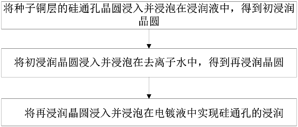
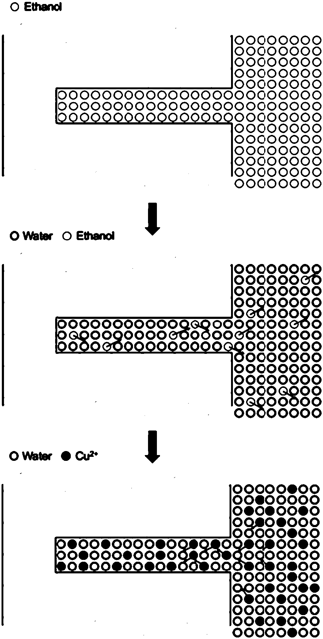
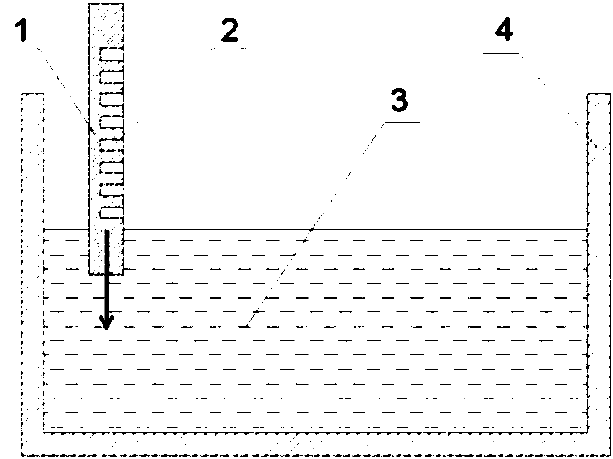
[0031] Such as figure 2 As shown, the TSV wafer of the seed copper layer is immersed vertically downward and immersed in the immersion solution, and the angle between the TSV wafer of the seed copper layer and the liquid surface of the immersion solution is 90°, as shown in image 3 As shown, the immersion speed of the TSV wafer with the seed copper layer is 5mm / s. When the TSV wafer with the seed copper layer is completely wetted, an incipient wetted wafer is obtained. Due to the high wetting property of ethanol to the seed copper (the contact angle is close to 0°), the ethanol will completely wet and fill the inside of the TSV. The TSVs have a pore diameter of 3 μm, a pore depth-to-diameter ratio of 15:1, and an immersion solution of absolute ethanol. Immerse the incipient wet wafer vertically downward and soak it in deionized water. Due to the miscibility of absolute ethanol and water in any ratio, the ethanol in the TSV will dissolve in the water, so that the deionized w...

Embodiment 2

[0033] Immerse the TSV wafer of the seed copper layer and soak it in the wetting solution. The angle between the TSV wafer of the seed copper layer and the liquid level of the immersion solution is 45°, such as Figure 4 As shown, the immersion speed of the TSV wafer with the seed copper layer is 5mm / s. When the TSV wafer with the seed copper layer is completely wetted, an incipient wetted wafer is obtained. Due to the high wetting property of ethanol to the seed copper (the contact angle is close to 0°), the ethanol will completely wet and fill the inside of the TSV. The TSVs have a pore diameter of 3 μm, a pore depth-to-diameter ratio of 15:1, and an immersion solution of absolute ethanol. Dip the incipient wet wafer into deionized water. Due to the miscibility of absolute ethanol and water in any ratio, the ethanol in the TSV will dissolve in the water, so that the deionized water can completely fill the TSV and clean the inside of the TSV. The included angle between the i...

Embodiment 3

[0035] Dip the TSV wafer of the seed copper layer vertically downwards and soak it in the immersion solution, the angle between the TSV wafer of the seed copper layer and the liquid level of the immersion solution is 0°, The immersion speed of the wafer is 5mm / s. When the TSV wafer of the seed copper layer is completely wetted, an incipient wetted wafer is obtained. Due to the high degree of wetting property (contact angle close to 0°) of the seed copper by ethanol, ethanol It will be possible to completely infiltrate and fill the interior of the TSV. The TSVs have a pore diameter of 3 μm, a pore depth-to-diameter ratio of 15:1, and an immersion solution of absolute ethanol. Immerse the incipient wet wafer vertically downward and soak it in deionized water. Due to the miscibility of absolute ethanol and water in any ratio, the ethanol in the TSV will dissolve in the water, so that the deionized water will completely fill the TSV, realizing the TSV Internal cleaning. The angl...


PUM

PropertyMeasurementUnit
pore sizeaaaaaaaaaa

Abstract

The invention discloses a three-step pre-wetting method of through-silicon-via plating. The method comprises a step of immersing a through-silicon-via wafer of a seed copper layer in an infiltration liquid and obtaining an initial wetted wafer when the through-silicon-via wafer of the seed copper layer is completely wetted, a step of immersing the initial wetted wafer into deionized water to obtain a re-wet wafer, and a step of immersing the re-wet wafer into an plating solution such that solute in the plating solution is diffused into a through silicon via to realize the internal infiltrationof the through silicon via. According to the method, the infiltration of the through silicon via with a higher depth-diameter ratio can be achieved, a problem of seed layer falling is not caused, thecost is reduced, the process time is greatly shortened, and the efficiency is improved.

Description

technical field [0001] The invention belongs to the field of 3D packaging, and more specifically relates to a three-step pre-wetting method for through-silicon hole electroplating. Background technique [0002] In through-silicon via plating, small-diameter TSVs (through-silicon vias) can support higher circuit densities. However, a smaller aperture means a higher aspect ratio. In addition, in order to be compatible with other 3D integration processes, the TSV plating process is often completed before wafer thinning, which means that the plating filling aspect ratio must exceed 10: 1 blind hole. Due to the surface tension of the electroplating solution, such a depth-to-diameter ratio will make it difficult for the plating solution to completely infiltrate the inside of the blind hole, which will result in pores in the blind hole after electroplating or even completely unable to fill. [0003] High vacuum can wet the higher aspect ratio, so for TSVs with high aspect ratio, ...

Claims


Application Information

Patent Timeline
Patent Type & Authority Applications(China)
IPC IPC(8): H01L21/768C25D7/12
CPCH01L21/76882C25D7/123
Inventor 李操费鹏刘胜
Owner HUAZHONG UNIV OF SCI & TECH
Learn More