Array substrate, fabrication method thereof and display device

A technology of array substrate and substrate substrate, which is applied in semiconductor/solid-state device manufacturing, instruments, semiconductor devices, etc., to avoid difficulty in climbing, reduce the area of ​​overlapping areas, and improve crosstalk.

Active Publication Date: 2018-03-27
BOE TECH GRP CO LTD +1
View PDF4 Cites 6 Cited by
  • Summary
  • Abstract
  • Description
  • Claims
  • Application Information

AI Technical Summary

Problems solved by technology

[0004] In view of this, in order to solve the problems of the prior art, the embodiments of the present invention provide an array substrate and its manufacturing method, and a display device. By improving the structure of the thin film transistor, the overlapping area between the data line and the gate line can be reduced Area, effectively improve the poor display problems such as crosstalk and flicker caused by the overlapping of data lines and gate lines; and, it can effectively reduce the risk of data line disconnection

Method used


Image

  • Array substrate, fabrication method thereof and display device
  • Array substrate, fabrication method thereof and display device
  • Array substrate, fabrication method thereof and display device

Examples


Embodiment 1

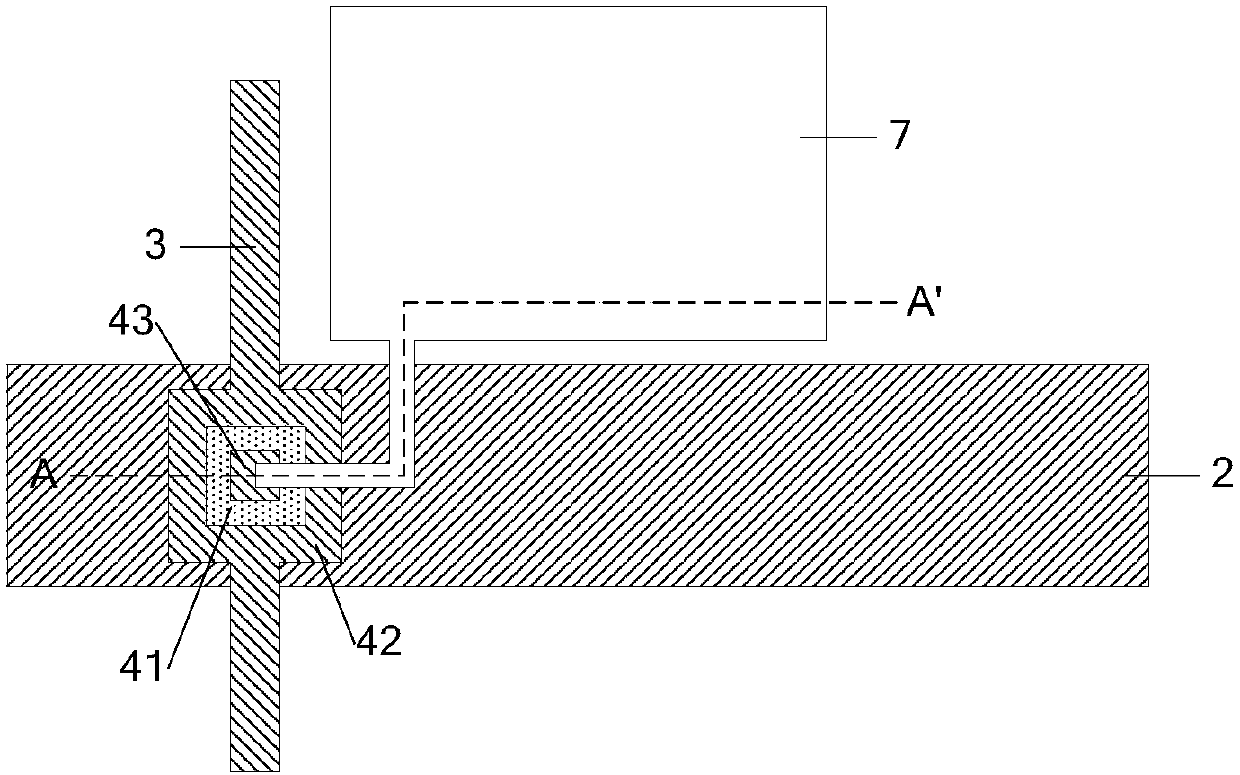
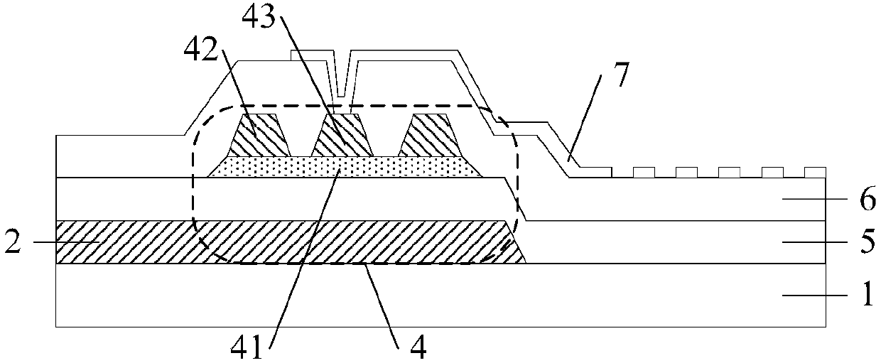
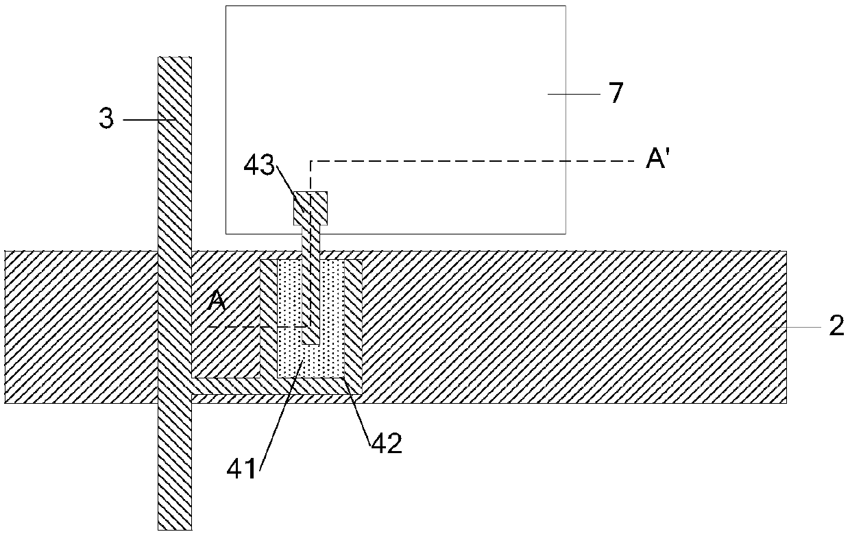
[0036] Such as figure 1 As shown, the embodiment of the present invention provides an array substrate, including: a base substrate 1 (not shown in the figure), intersecting gate lines 2 and data lines 3 arranged above the base substrate 1, and thin film transistors 4 The thin film transistor 4 includes: a gate, an active layer 41 disposed on the side of the gate away from the base substrate 1, and a source 42 and a drain 43 disposed on the side of the active layer 41 away from the base substrate 1; The gate of 4 is a part of the gate line 2; the source 42 is a part of the data line 3, and at least part of the area of ​​the source 42 is located in the area where the orthographic projection of the data line 3 and the gate line 2 on the base substrate 1 overlaps. .

[0037]It should be noted that, first, if figure 2 As shown, the above-mentioned array substrate certainly also includes a gate insulating layer 5 disposed to cover the gate lines 2 , and the specific structure can...

Embodiment 2

[0061] An embodiment of the present invention also provides a method for preparing the above-mentioned array substrate, which includes: sequentially forming a gate line, a gate insulating layer, an active layer, a data line, and a drain on the base substrate; wherein, A part of the gate line is used as the gate, the active layer is formed on the top of the gate, and the drain is formed on the active layer; a part of the data line is used as the source, and at least part of the source area is located between the data line and the gate line. The orthographic projection on the substrate exists in an overlapping area; the gate, active layer, source and drain form a thin film transistor (Thin Film Transistor, TFT).

[0062] Wherein, the step of forming the data line and the drain electrode includes: sequentially forming a metal layer and a photoresist layer on the base substrate on which the gate line, the gate insulating layer and the active layer are formed; Exposure and developm...

Embodiment 3

[0082] On the basis of the above, an embodiment of the present invention further provides a display device, including the above-mentioned array substrate. The display device may specifically be a liquid crystal display device, and may be a product or component with any display function such as a liquid crystal display, a liquid crystal TV, a digital photo frame, a mobile phone, a tablet computer, a navigator, and the like.


PUM


Abstract

The invention provides an array substrate, a fabrication method thereof and a display device. By improving a structure of a thin film transistor, the overlapped regional area between a data line and agate line can be reduced, the unfavorable problem of display such as crosstalk and flicker caused by overlapping of the data line and the gate line is effectively improved, and the risk that the dataline is open can be effectively reduced. The array substrate comprises a substrate, a gate line, a data line and a thin film transistor, wherein the gate line and the data line are arranged above thesubstrate in a staggered way, the thin film transistor comprises a gate, an active layer, a source and a drain, the active layer is arranged at one side, far away from the substrate, of the gate, thesource and the drain are arranged at one side, far away from the substrate, of the active layer, the gate is a part of the gate line, the source is a part of the data line, and at least one part of region of the source is arranged in a region where positive projections of the data line and the gate line on the substrate are overlapped.

Description

technical field [0001] The present invention relates to the field of display technology, in particular to an array substrate, a preparation method thereof, and a display device. Background technique [0002] In the array substrate, gate lines (Gate Lines) and data lines (Data Lines) on different layers are intersected and overlap each other, and parasitic capacitance will be generated between the upper and lower layer metals in the overlapping area, causing each Signals on metal traces create crosstalk. With the increase of the display area of ​​the display device, the metal traces used on the large-scale array substrate are longer, and the crosstalk will cause the signal delay on the gate line and the data line, such as Crosstalk (crosstalk), Flicker (flicker) etc. display bad. [0003] In addition, because in the array substrate, the gate lines are usually located below the data lines, and there is a problem that the data lines need to climb over the gate lines at the in...

Claims


Application Information

Patent Timeline
Patent Type & Authority Applications(China)
IPC IPC(8): H01L27/12H01L21/77G02F1/1368G02F1/1362
CPCG02F1/136286G02F1/1368H01L27/1214H01L27/124H01L27/1259H01L29/41733G02F1/134372G02F1/133345
Inventor 刘耀陈曦廖加敏李宗祥
Owner BOE TECH GRP CO LTD
Why Eureka
Try Eureka