

Display device
A technology for display devices and substrates, applied in identification devices, lighting devices, instruments, etc., can solve problems such as display image quality degradation, color bleeding, and resolution reduction, and achieve the effect of suppressing quality degradation
- Summary
- Abstract
- Description
- Claims
- Application Information
AI Technical Summary
Problems solved by technology
Method used
Image

Examples
example 1
[0031] 2. Example 1 (display device according to first aspect of the present disclosure)
example 2
[0032] 3. Example 2 (display device according to second aspect of the present disclosure)
[0033] 4. Example 3 (variation of Example 1 and Example 2)
[0034] 5. Other
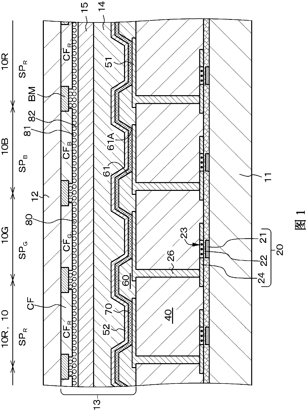
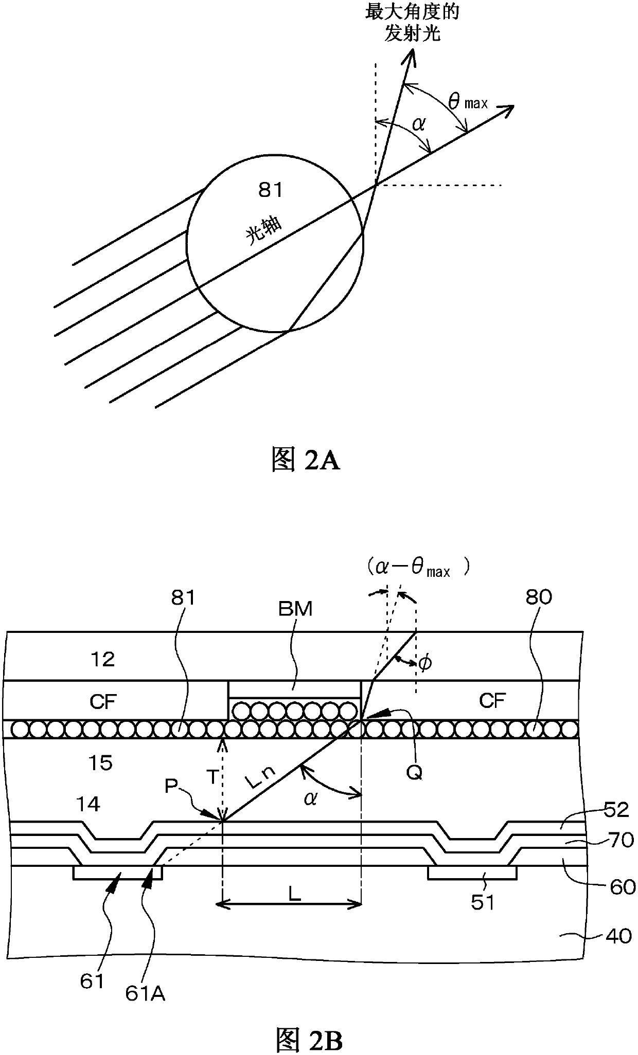
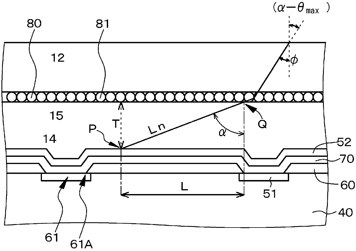
[0035]
[0036] In the display device according to the first aspect of the present disclosure, the particle is spherical and considered as a spherical lens (the display device according to the first aspect of the present disclosure), or the protrusion is considered as a part of the spherical lens (according to the present disclosure The display device of the second aspect). When parallel rays are incident on the spherical lens and emitted from the spherical lens, if the maximum value (maximum angle) of the angle formed by the optical axis of the spherical lens and the rays emitted from the spherical lens is given by θ max represents, then the average distance between the second electrode and the light-diffusing layer is represented by T, the shortest distance between adjacent light-emitting elements is re...
example 3
[0152] Example 3 is a variation of Examples 1 and 2. In Example 3, a light reflection layer was formed under the first electrode via an interlayer insulating layer, and a resonator structure was formed between the light reflection layer and the second electrode. Figure 5 A schematic partial sectional view of the display device of Example 3 obtained by modifying the display device of Example 1 is shown. also, Image 6 A schematic partial cross-sectional view of the display device of Example 3 obtained by modifying the display device of Example 2 is shown.
[0153] Each of the light-emitting elements 10 of Example 3 includes a lower layer / interlayer insulating layer 31, a light reflective layer 37 formed on the lower layer / interlayer insulating layer 31, an upper layer / layer covering the lower layer / interlayer insulating layer 31 and the light reflective layer 37. The interlayer insulating layer 32, the first electrode 51 formed on the upper layer / interlayer insulating layer ...
PUM
 Abstract
Description
Claims
Application Information