
A method for improving the efficiency of cross-page storage address mapping in nand flash memory

A storage address and flash memory technology, which is applied in the field of improving the efficiency of cross-page storage address mapping in NAND flash memory, can solve the problems of large information bit address mapping space and low space utilization, and achieve the effect of reducing storage space and being easy to implement

Active Publication Date: 2020-06-02
HUAZHONG UNIV OF SCI & TECH
View PDF5 Cites 0 Cited by
  • Summary
  • Abstract
  • Description
  • Claims
  • Application Information

AI Technical Summary

Problems solved by technology

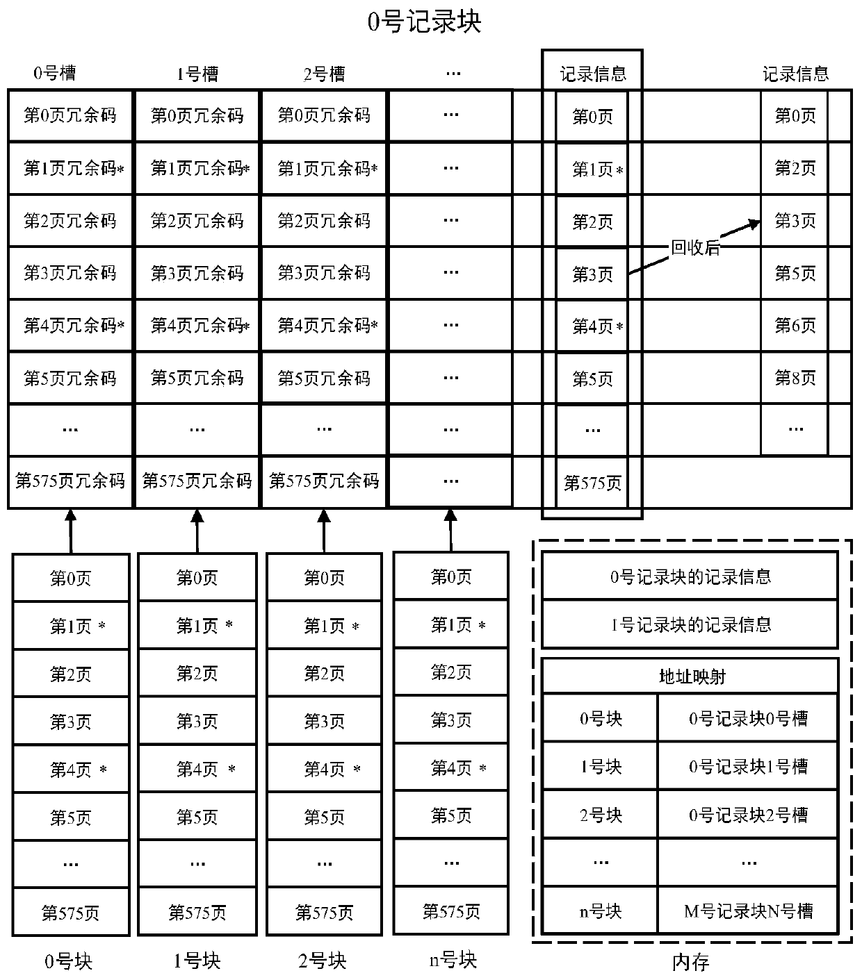
[0005] In view of the above defects or improvement needs of the prior art, the present invention provides a method for improving the efficiency of cross-page storage address mapping in NAND flash memory. The technical problem of low space utilization caused by large mapped space

Method used


Image

  • A method for improving the efficiency of cross-page storage address mapping in nand flash memory
  • A method for improving the efficiency of cross-page storage address mapping in nand flash memory

Examples


Embodiment Construction

[0027] In order to make the object, technical solution and advantages of the present invention clearer, the present invention will be further described in detail below in conjunction with the accompanying drawings and embodiments. It should be understood that the specific embodiments described here are only used to explain the present invention, not to limit the present invention. In addition, the technical features involved in the various embodiments of the present invention described below can be combined with each other as long as they do not constitute a conflict with each other.

[0028] Below at first technical terms of the present invention are explained and illustrated:

[0029] Chip (Die): A chip is a small square on a wafer. Several chips may be packaged in one chip. Due to the different processes and technologies of flash memory, the concept of a chip is born. The common ones are Mono chip and A chip. , B chip, etc.

[0030] Group (Plane): A group is the smallest ...


PUM


Abstract

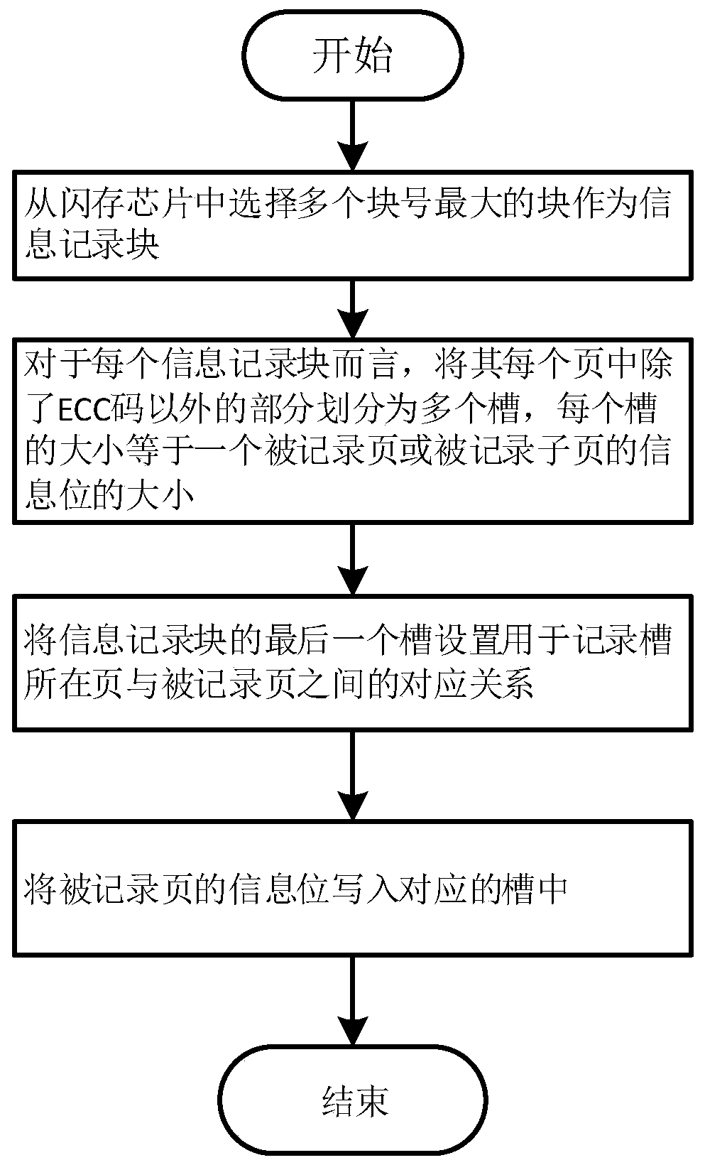
The invention discloses a method for improving the cross-page storage address mapping efficiency in a NAND flash memory. The method comprises the steps that multiple blocks with the largest block number are selected from the flash memory to serve as information recording blocks, for each information recording block, the parts, except for ECC codes, in each page are divided into multiple slots, thesize of each slot is equal to that of an information bit of a recorded page or a recorded sub-page, the last slot of each information recording block is arranged to be used for recording a corresponding relationship between the page where the slot is located and the recorded page, and the information bit of the recorded page is written into the corresponding slot. Accordingly, the space-efficientsmall-capacity information bit cross-page storage address mapping method is provided according to research and engineering demands on flash memory structure distribution, reading and writing processes and other characteristics.

Description

technical field [0001] The invention belongs to the field of computer storage, and more specifically relates to a method for improving the efficiency of cross-page storage address mapping in NAND flash memory. Background technique [0002] With the development of flash memory technology, 3D TLC has become a hot spot for future application and research due to its advantages of high capacity and low cost. However, due to the high original bit error rate of 3D TLC, LDPC decoding algorithm must be used for error correction, but the hardware design of LDPC decoder is complex and the decoding delay is high, many researchers hope to optimize and improve it . [0003] The method for optimizing the decoding algorithm that is usually used at present needs to set information bits in the out-of-band (Out of band, OOB) space. If the information bits are too long, these information bits need to be stored in a fixed block in the flash memory. Then a mapping relationship between the origi...

Claims


Application Information

Patent Timeline
Patent Type & Authority Patents(China)
IPC IPC(8): G06F12/02G06F12/0802
CPCG06F12/0246G06F12/0802
Inventor 吴非谢长生刘伟华张猛
Owner HUAZHONG UNIV OF SCI & TECH
Learn More