Voltage compensation device, voltage compensation method and display device

A voltage compensation and display device technology, applied to static indicators, instruments, etc., to achieve the effect of improving image display quality, less time-consuming, and high efficiency

Active Publication Date: 2018-03-30
BOE TECH GRP CO LTD
View PDF10 Cites 9 Cited by
  • Summary
  • Abstract
  • Description
  • Claims
  • Application Information

AI Technical Summary

Problems solved by technology

[0006] In view of the above problems, the present invention proposes a voltage compensation device, a voltage compensation method and a

Method used


Image

  • Voltage compensation device, voltage compensation method and display device
  • Voltage compensation device, voltage compensation method and display device
  • Voltage compensation device, voltage compensation method and display device

Examples


Embodiment 1

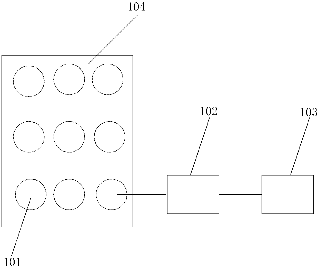
[0044] An embodiment of the present invention provides a voltage compensation device. The schematic diagram of the voltage compensation device is shown in figure 1 As shown, the voltage compensation device specifically includes the following components: a thermal sensor group 101 , a processor 102 and a power management module 103 .

[0045] Both the thermal sensor group 101 and the power management module 103 are electrically connected to the processor 102 .

[0046] The thermal sensor group 101 is disposed at a corresponding position of the pixel unit.

[0047] The processor 102 is configured to determine the actual pixel voltage of the pixel unit corresponding to the thermal sensor group 101 according to the temperature electrical signal when receiving the temperature electrical signal fed back by the thermal sensor group 101; The difference between the reference pixel voltages of the pixel unit determines the compensated data signal and sends it to the power management m...

Embodiment 2

[0053] Based on the same inventive concept, an embodiment of the present invention also provides a display device, the structural diagram of which is shown in figure 1 shown, including:

[0054] The display panel 104 includes any voltage compensation device as provided in the above-mentioned embodiments of the present invention. The pixel units in the display panel 104 include organic light emitting diodes (OLEDs), and the thermal sensor group 101 is disposed at corresponding positions of the organic light emitting diodes.

[0055] The beneficial effect obtained by using the display device provided by the embodiment of the present invention to perform the voltage compensation of the pixel unit is consistent with the aforementioned voltage compensation device provided by the embodiment of the present invention, which will not be repeated here.

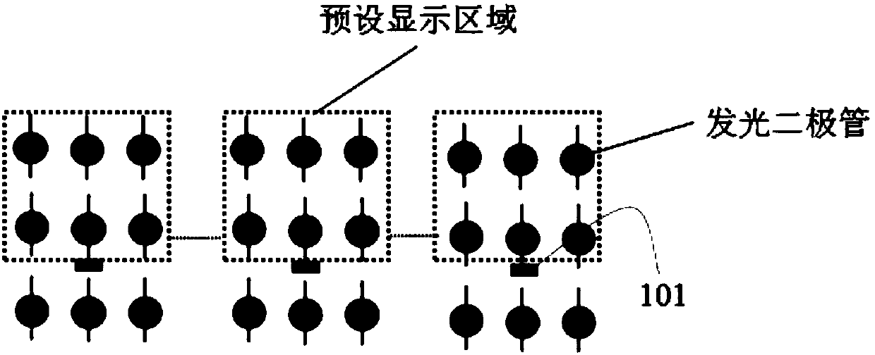
[0056] In a specific implementation manner, the thermal sensor group in the embodiment of the present invention includes a plurality o...

Embodiment 3

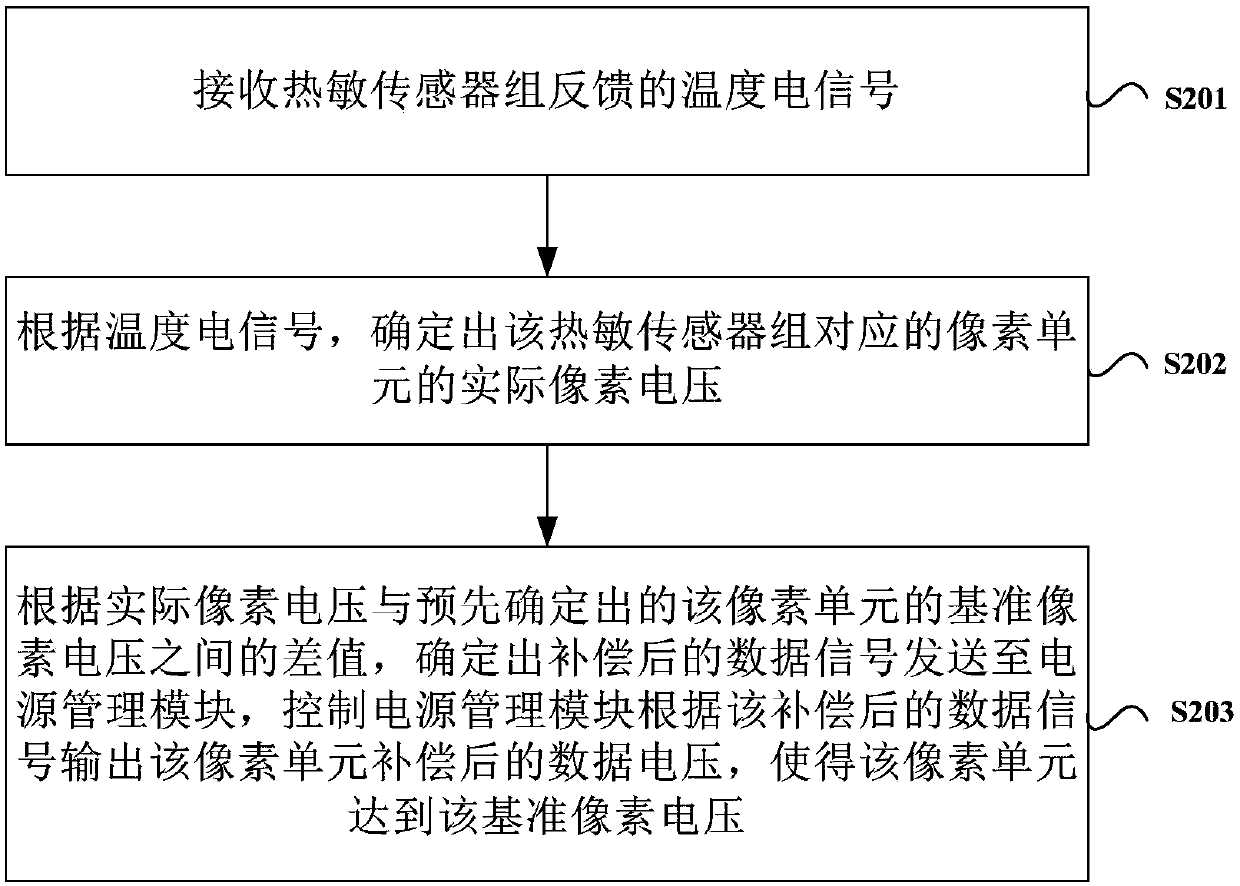
[0060] Based on the voltage compensation device or the display device provided by the above embodiments of the present invention, the embodiments of the present invention further provide a voltage compensation method. The specific flowchart of the voltage compensation method is as follows: image 3 As shown, it specifically includes the following steps:

[0061] S201: Receive a temperature electrical signal fed back by the thermal sensor group.

[0062] S202: Determine the actual pixel voltage of the pixel unit corresponding to the thermal sensor group according to the electrical temperature signal.

[0063] S203: According to the difference between the actual pixel voltage and the predetermined reference pixel voltage of the pixel unit, determine the compensated data signal and send it to the power management module, and control the power management module to output the The compensated data voltage of the pixel unit makes the pixel unit reach the reference pixel voltage.

...


PUM


Abstract

The invention provides a voltage compensation device, a voltage compensation method and a display device. The voltage compensation device comprises a heat-sensitive sensor group, a processor and a power management module, wherein the heat-sensitive sensor group and the power management module are electrically connected with the processor, and the heat-sensitive sensor group is arranged at a position corresponding to a pixel unit. By cooperative work of the heat-sensitive sensor group, the processor and the power management module, the power management module is controlled to output data voltage compensated by the pixel unit based on temperature information corresponding to the pixel unit and detected by the heat-sensitive sensor group, so that the pixel unit reaches reference pixel voltage. Compared with a method for compensating voltage by sensing electrical or optical characteristics of pixels through equipment in the prior art, time consumed for detecting the temperature informationcorresponding to the pixel unit is less, the voltage compensation efficiency of the pixel unit is high, the cost of the heat-sensitive sensor group is lower than that of the pixel sensing equipment,and large-area production can be realized.

Description

technical field [0001] The present invention relates to the display field, specifically, the present invention relates to a voltage compensation device, a voltage compensation method and a display device. Background technique [0002] At present, compared with LCD (liquid crystal display panel), AMOLED (active matrix organic light-emitting diode panel) has many advantages such as high contrast, ultra-thin, and bendable, and has attracted widespread attention from users. [0003] Although the current development of AMOLED is relatively mature, there are still some shortcomings. For example, brightness uniformity and image retention are the two main issues it currently faces. Specifically, under long-term pressurization and high temperature, the threshold voltage of each region in the display panel will drift. Due to the different display screens, the threshold voltage drift of each region in the display panel is also different, resulting in the display of each region in the ...

Claims


Application Information

Patent Timeline
IPC IPC(8): G09G3/3225
CPCG09G3/3225G09G2320/02G09G3/3208G09G2320/029G09G2320/041G09G2330/021G09G2330/028G09G2320/0257
Inventor 黄建邦石领王丽
Owner BOE TECH GRP CO LTD
Why Eureka
Try Eureka