Internal connection structure of semiconductor device and manufacturing method of internal connection structure

A technology of interconnect structure and manufacturing method, which is applied in semiconductor/solid-state device manufacturing, semiconductor devices, semiconductor/solid-state device components, etc., and can solve problems such as interconnection crosstalk

Pending Publication Date: 2018-04-10
CHANGXIN MEMORY TECH INC
View PDF8 Cites 4 Cited by
  • Summary
  • Abstract
  • Description
  • Claims
  • Application Information

AI Technical Summary

Problems solved by technology

The continuous reduction in the size of semiconductor devices and the size of interconnection lines leads to the gradual reduction of the spacing between interconnection lines, w

Method used


Image

  • Internal connection structure of semiconductor device and manufacturing method of internal connection structure
  • Internal connection structure of semiconductor device and manufacturing method of internal connection structure
  • Internal connection structure of semiconductor device and manufacturing method of internal connection structure

Examples


Embodiment Construction

[0050] The interconnection structure and manufacturing method of the semiconductor device proposed by the present invention will be further described in detail below with reference to the accompanying drawings and specific embodiments. Advantages and features of the present invention will be apparent from the following description and claims. It should be noted that all the drawings are in a very simplified form and use imprecise scales, and are only used to facilitate and clearly assist the purpose of illustrating the embodiments of the present invention. In addition, the structures shown in the drawings are often a part of the actual structures. In particular, each drawing needs to display different emphases, and sometimes uses different scales.

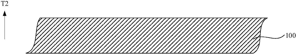
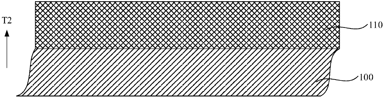
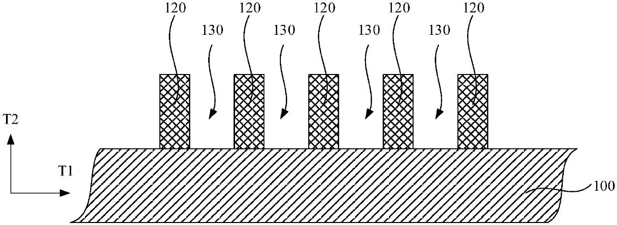
[0051] Specifically, please refer to Figure 1 to Figure 7 ,in, figure 1 is a schematic cross-sectional view of the substrate provided in the method for manufacturing the interconnection structure of the semiconductor device acc...


PUM


Abstract

The invention provides an internal connection structure of a semiconductor device and a manufacturing method of the internal connection structure. The manufacturing method includes the steps of forming a first medium layer on the substrate structure and covering a first layer interconnecting wire in the process of forming the inner connecting layer, wherein the first medium layer is attached to the side wall of the first layer interconnecting wire and grows in the direction away from the side wall of the first layer interconnecting wire to partially fill the interval region in a non-filling mode, so that a first air gap is formed in the first medium layer in the interval region, and the first air gap is sealed in the first medium layer; opening the first air gap to form a plurality of opengrooves between the first layer interconnecting wires, and expanding the space size of the grooves; forming a second medium layer on the first medium layer, covering the upper notch of the grooves bythe second medium layer to seal the open slot to form a second air gap, wherein the space enclosed by the second air gap is larger than the space enclosed by the first air gap, so that an air gap with a larger size can be formed between every two adjacent interconnecting wires to realize effective and reliable isolation between the interconnecting wires.

Description

technical field [0001] The invention relates to the technical field of semiconductor manufacturing, in particular to an interconnection structure of a semiconductor device and a manufacturing method thereof. Background technique [0002] With the continuous development of semiconductor integrated circuit technology, interconnection structures for connecting semiconductor devices are more and more widely used. The interconnection structures mainly include interconnection lines and dielectric layers for isolating the interconnection lines. The continuous reduction in the size of semiconductor devices and the size of interconnection lines leads to the gradual reduction of the spacing between interconnection lines, which in turn causes the part of the dielectric layer between the interconnection lines to become smaller and smaller, which often leads to interconnection Crosstalk occurs between wires. At present, by reducing the dielectric constant of the dielectric layer, this c...

Claims


Application Information

Patent Timeline
IPC IPC(8): H01L21/768H01L23/528
CPCH01L23/528H01L21/7682
Inventor 不公告发明人
Owner CHANGXIN MEMORY TECH INC
Why Eureka
Try Eureka