Method for reducing RC delay of integrated circuit

A technology for integrated circuits and low dielectric constant materials, which is applied in the field of reducing the RC delay of integrated circuits, and can solve the problems of increasing the k value and large k value of the latter dielectric material

Inactive Publication Date: 2014-11-05
SHANGHAI HUALI MICROELECTRONICS CORP
View PDF3 Cites 1 Cited by
  • Summary
  • Abstract
  • Description
  • Claims
  • Application Information

AI Technical Summary

Problems solved by technology

NDC films can well block copper diffusion, but compared with low dielectric constant materials (k=2.0-3.0), its k value is too large (about 5.3), which will undoubtedly increase the overall k value of the latter dielectric material

Method used


Image

  • Method for reducing RC delay of integrated circuit
  • Method for reducing RC delay of integrated circuit
  • Method for reducing RC delay of integrated circuit

Examples


Embodiment Construction

[0016] In order to make the content of the present invention clearer and easier to understand, the content of the present invention will be described in detail below in conjunction with specific embodiments and accompanying drawings.

[0017] Figure 2 to Figure 6 Each step of the method for reducing the RC delay of an integrated circuit according to a preferred embodiment of the present invention is schematically shown.

[0018] Specifically, as Figure 2 to Figure 6 As shown, the method for reducing the RC delay of an integrated circuit according to a preferred embodiment of the present invention includes:

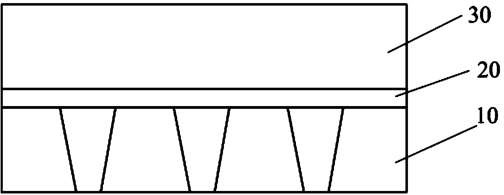
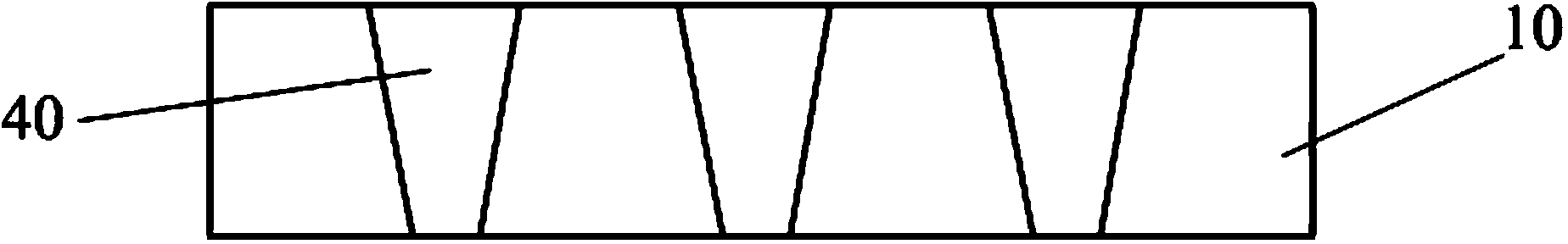
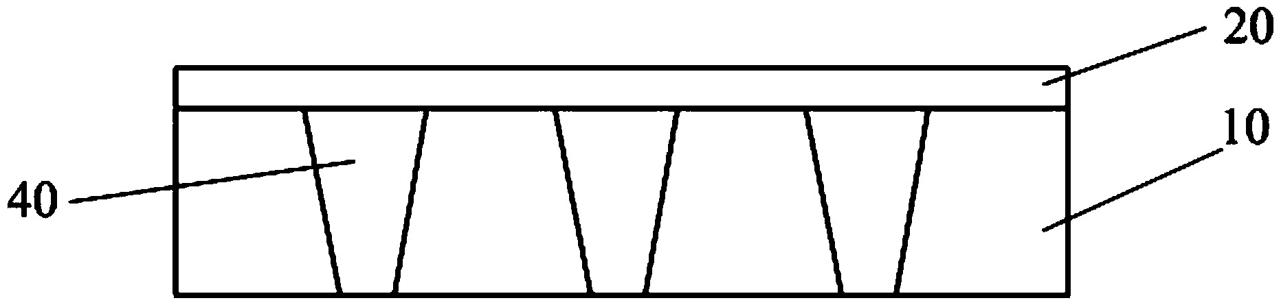
[0019] A copper interconnection structure 40 is formed in the porous low dielectric constant material 10, and the copper interconnection structure 40 is subjected to chemical mechanical polishing planarization treatment, such as figure 2 shown; for example, low-k materials have a k between 2.0-3.0.

[0020] A copper diffusion dielectric barrier layer (for example, a ...


PUM


Abstract

The invention provides a method for reducing the RC delay of an integrated circuit. The method includes the steps that a copper interconnecting structure is formed in porous low dielectric constant material, and chemical and mechanical grinding flattening processing is performed on the copper interconnecting structure; a copper diffusion dielectric barrier layer grows on the surface of the porous low dielectric constant material for the copper interconnection structure; the portion, outside the copper interconnecting structure, of the copper diffusion dielectric barrier layer is removed through the photoetching and etching process, and the portion, on the copper interconnecting structure, of the copper diffusion dielectric barrier layer is reserved; the low dielectric constant material grows again, and therefore an upper porous low dielectric constant material layer is formed on the reserved copper diffusion dielectric barrier layer and the porous low dielectric constant material; and the surface of the upper porous low dielectric constant material layer is processed in a flattening mode.

Description

technical field [0001] The invention relates to the field of semiconductor manufacturing, and more specifically, the invention relates to a method for reducing the RC delay of an integrated circuit. Background technique [0002] With the continuous reduction of the feature size of semiconductor integrated circuits, the delay of the back-end interconnection resistance capacitor (RC) shows a significant increase trend. In order to reduce the RC delay, low dielectric constant materials are introduced, and copper interconnection replaces aluminum interconnection. Even become the mainstream technology. [0003] Nitrogen-doped silicon carbide (NDC) film is used as a barrier layer in the back-end process of integrated circuit manufacturing. The purpose is to prevent direct contact between copper and dielectric materials, and copper diffusion occurs, resulting in device failure. Usually after Cu CMP (Chemical Mechanical Polishing), before low-k dielectric material deposition (e.g. ...

Claims


Application Information

Patent Timeline
Patent Type & Authority Applications(China)
IPC IPC(8): H01L21/768H01L23/522
CPCH01L21/7684H01L21/76819H01L23/522
Inventor 雷通桑宁波
Owner SHANGHAI HUALI MICROELECTRONICS CORP
Why Eureka
Try Eureka