Integration technology of copper and low K dielectric material

A dielectric material and process technology, which is applied in the field of integration technology of copper and low-K dielectric materials, can solve problems such as difficult to achieve effective integration of copper and low-K dielectric materials, increase of K value of dielectric materials, damage of dielectric materials, etc., to achieve improved Hole rate, reduce K value, avoid damage effect

Inactive Publication Date: 2016-02-10
ACM RES SHANGHAI
View PDF3 Cites 1 Cited by
  • Summary
  • Abstract
  • Description
  • Claims
  • Application Information

AI Technical Summary

Problems solved by technology

However, curing the low-K dielectric layer by UV curing process will lead to an increase in the K value of the dielectric material
In addition, the above-mentioned integration process uses chemical mechanical planarization technology to remove the copper layer and barrier layer on the surface. The technical characteristics of chemical mechanical planarization itself determine that the K value of the dielectric material cannot be too low, otherwise, the chemical mechanical planarization process. Downforce will cause damage to the dielectric material. Therefore, the above integration process has limitations, and it is difficult to achieve effective integration of copper and low-K dielectric materials.

Method used


Image

  • Integration technology of copper and low K dielectric material
  • Integration technology of copper and low K dielectric material
  • Integration technology of copper and low K dielectric material

Examples


Embodiment Construction

[0025] In order to describe the technical content, achieved goals and effects of the present invention in detail, the following will be described in detail in conjunction with the embodiments and accompanying drawings.

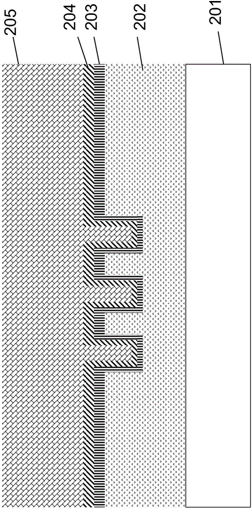
[0026] refer to image 3 and combine figure 2 As shown, an integration process of copper and low-K dielectric material disclosed by the present invention includes the following steps:

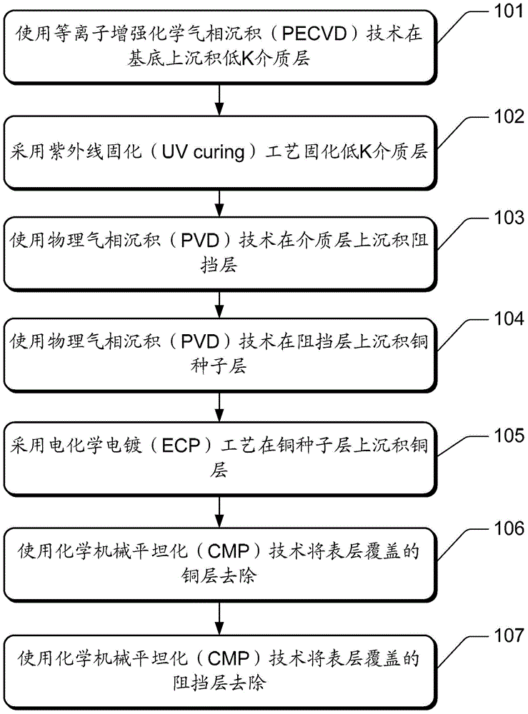
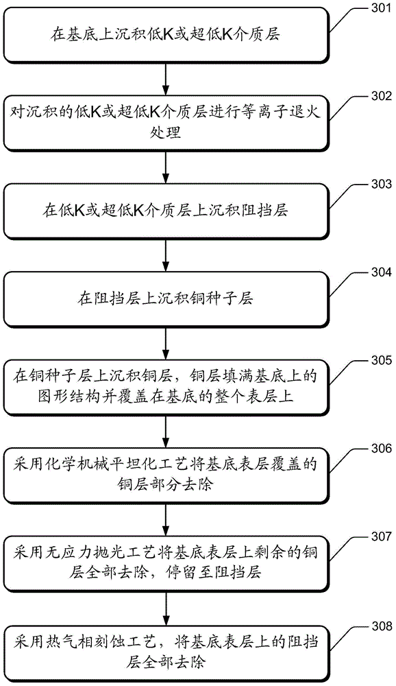
[0027] Step 301: Deposit a low-K or ultra-low-K dielectric layer 202 on the substrate 201, the K value of the low-K dielectric layer is less than 2.5, and the K value of the ultra-low-K dielectric layer is less than 2. Specifically, a low-K or ultra-low-K dielectric layer 202 is deposited on the substrate 201 by plasma enhanced chemical vapor deposition (PECVD), and the low-K or ultra-low-K dielectric layer 202 contains a sacrificial porogen.

[0028] Step 302: Perform plasma annealing (Plasma Anneal) on the deposited low-K or ultra-low-K dielectric layer 202, specifically, ...


PUM

PropertyMeasurementUnit
Wavelengthaaaaaaaaaa

Abstract

The invention discloses an integration technology of copper and a low K dielectric material. The method comprises the following steps of depositing a low K or ultralow K dielectric layer on a substrate; carrying out plasma annealing processing on the deposited low K or ultralow K dielectric layer; depositing a barrier layer on the low K or ultralow K dielectric layer; depositing a copper seed layer on the barrier layer; depositing a copper layer on the copper seed layer, wherein the copper layer fills in a graph structure on the substrate and covers a whole surface layer of the substrate; using a chemical mechanical planarization technology to remove a copper layer portion on the substrate surface layer; using a stress-free polishing technology to completely remove the residual copper layer on the substrate surface layer and staying at the barrier layer; using a hot gas phase etching technology to completely remove the barrier layer on the substrate surface layer. By using the technology of the invention, the dielectric material can maintain an enough low K value and integration with copper is realized, and a technical barrier in the prior art is broken through.

Description

technical field [0001] The invention relates to the field of integrated circuit manufacturing, in particular to an integration process of copper and low-K dielectric materials, which is used to reduce the resistance-capacitance hysteresis of integrated circuits. Background technique [0002] With the continuous progress of integrated circuit technology, chips with high speed, high device density, low power consumption and low cost have become the mainstream products of VLSI. At this time, the density of wires in the chip continues to increase, the width and spacing of wires continue to shrink, and the parasitic effects produced by the resistance R and capacitance C in the interconnection structure become more and more obvious. In order to overcome the signal propagation delay caused by resistance-capacitance hysteresis (RCdelay), inter-line interference and power dissipation, etc., copper wires replace traditional aluminum wires and become the development direction of integr...

Claims


Application Information

Patent Timeline
IPC IPC(8): H01L21/768H01L21/3105
Inventor 金一诺王坚王晖
Owner ACM RES SHANGHAI
Why Eureka
Try Eureka