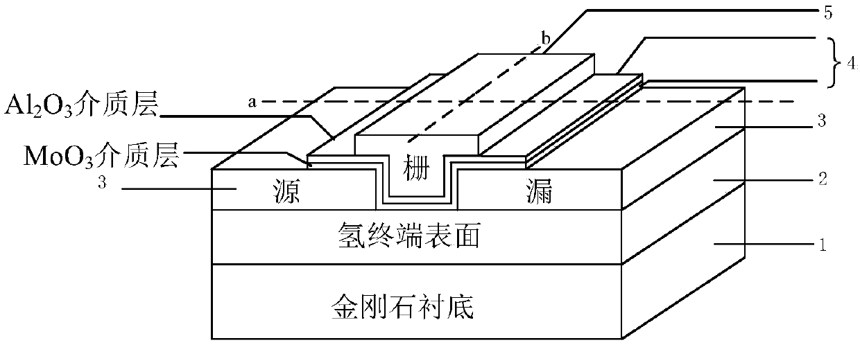
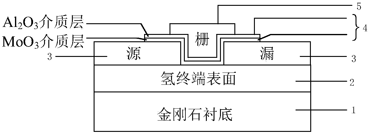
MoO3/Al2O3 double-layer gate medium based diamond field effect transistor with zero gate-source distance and manufacturing method of field effect transistor
A field effect transistor, diamond technology, applied in transistors, semiconductor/solid state device manufacturing, semiconductor devices, etc., can solve the problem of not increasing the current, achieve high density and mobility, reduce gate leakage, and reduce conduction. The effect of resistance
- Summary
- Abstract
- Description
- Claims
- Application Information
AI Technical Summary
Problems solved by technology
Method used
Image


Examples
Embodiment 1
[0034] Embodiment 1: making substrate is single crystal diamond, MoO 3 The thickness of the gate dielectric layer is 5nm, Al 2 o 3 A double-layer gate dielectric field effect transistor with a gate dielectric layer thickness of 5nm:
[0035] Step 1: Generate a hydrogen terminated surface on a single crystal diamond substrate.
[0036]Place the single crystal diamond substrate in the hydrogen plasma in the reaction chamber, flow into the reaction chamber a hydrogen gas with a flow rate of 500 sccm, set the pressure at 80 mbar, and stop for 5 minutes at a temperature of 800 ° C to generate on the diamond substrate hydrogen-terminated surface, the result is as Figure 4 (a).
[0037] Step 2: Grow a gold film on the surface of the hydrogen terminal.
[0038] A gold film with a thickness of 80nm is deposited on the surface of the hydrogen terminal by thermal evaporation process as a protective layer on the surface of the hydrogen terminal. The growth results are as follows: ...
Embodiment 2
[0048] Embodiment 2: making substrate is polycrystalline diamond, MoO 3 The thickness of the gate dielectric layer is 10nm, Al 2 o 3 A double-layer gate dielectric field effect transistor with a gate dielectric layer thickness of 15nm.
[0049] Step 1: Generating a hydrogen-terminated surface on a polycrystalline diamond substrate.
[0050] The single crystal diamond substrate is placed in the hydrogen plasma in the reaction chamber, the flow rate of 700sccm hydrogen gas is introduced into the reaction chamber, the pressure is set at 100mbar, and the temperature is 850°C, stop for 15min to generate on the diamond substrate hydrogen-terminated surface, the result is as Figure 4 (a).
[0051] Step 2: growing a gold film on the surface of the hydrogen terminal.
[0052] A layer of 100nm Au was deposited on the surface of hydrogen termination by thermal evaporation process to protect the surface of hydrogen termination. The results are as follows Figure 4 (b).
[0053] St...
Embodiment 3
[0062] Embodiment 3: making substrate is single crystal diamond, MoO 3 The thickness of the gate dielectric layer is 40nm, Al 2 o 3 Zero-gate-source pitch field effect transistor with a gate dielectric layer thickness of 50nm:
[0063] Step A: Place the single crystal diamond substrate in the hydrogen plasma in the reaction chamber, feed hydrogen gas with a flow rate of 1000sccm into the reaction chamber, set the pressure at 150mbar, and stop for 30min at a temperature of 950°C, so that the diamond A hydrogen-terminated surface is generated on the substrate, and the results are as follows Figure 4 (a).
[0064] Step B: Deposit a 180nm-thick gold film on the surface of the hydrogen terminal using electron beam evaporation technology to protect the surface of the hydrogen terminal. The results are as follows Figure 4 (b).
[0065] Step C: Spin-coat photoresist on the gold film, use a photolithography machine to expose, make an isolation area pattern, and then use a wet et...
PUM
 Abstract
Description
Claims
Application Information
 - R&D
- Intellectual Property
- Life Sciences
- Materials
- Tech Scout
- Unparalleled Data Quality
- Higher Quality Content
- 60% Fewer Hallucinations
Browse by: Latest US Patents, China's latest patents, Technical Efficacy Thesaurus, Application Domain, Technology Topic, Popular Technical Reports.
© 2025 PatSnap. All rights reserved.Legal|Privacy policy|Modern Slavery Act Transparency Statement|Sitemap|About US| Contact US: help@patsnap.com