A test method for bias temperature instability applied to MOS devices

A MOS device, instability technology, applied in the direction of single semiconductor device testing, instrumentation, measuring electricity, etc., can solve the problem of inaccurate testing of bias temperature instability

Active Publication Date: 2020-06-09
GUILIN UNIV OF ELECTRONIC TECH
View PDF7 Cites 0 Cited by
  • Summary
  • Abstract
  • Description
  • Claims
  • Application Information

AI Technical Summary

Problems solved by technology

[0004] The technical problem to be solved by the present invention is the inaccurate technical problem of the bias temperature instability test existing in the prior art, and a new test method for the bias temperature instability of the MOS device is provided, and the technical method has the advantages of accurate test technical characteristics of

Method used


Image

  • A test method for bias temperature instability applied to MOS devices
  • A test method for bias temperature instability applied to MOS devices

Examples


Embodiment 1

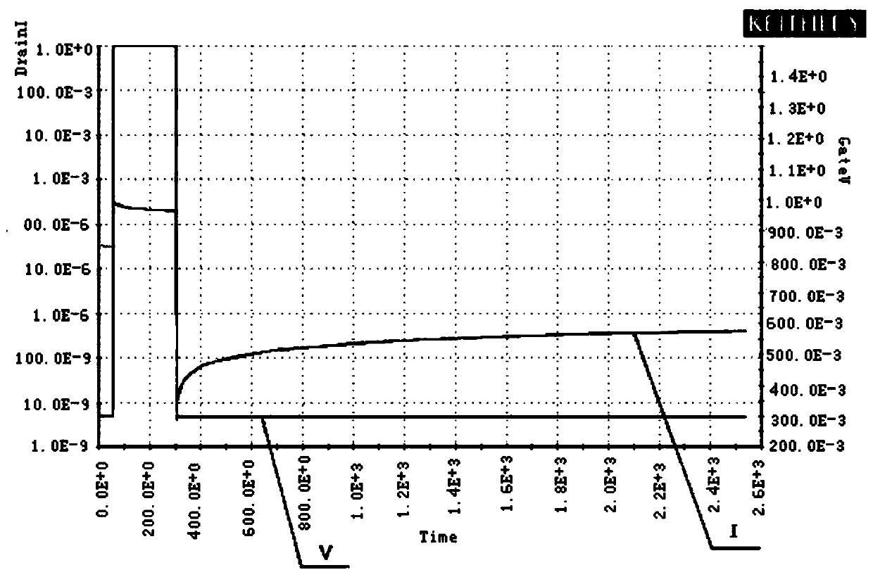
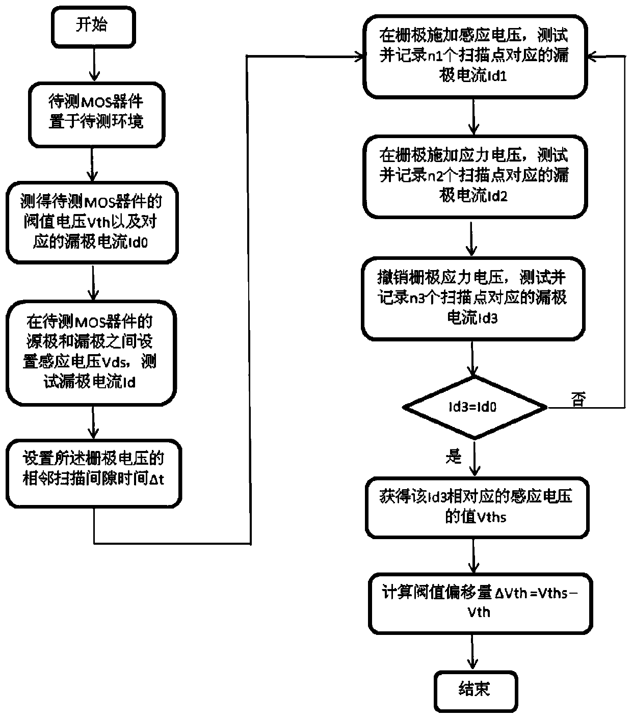
[0028] like figure 1 and figure 2 As shown, this embodiment provides a method for testing bias temperature instability applied to MOS devices, comprising the following steps:

[0029] 1. Place the MOS device to be tested in the test environment, scan the gate voltage from -1V to 1V, scan to obtain the original transfer characteristic curve of the MOS device to be tested, adjust the gate voltage, according to the original transfer characteristic curve It is determined that the MOS device to be tested is in a normal working state, and the threshold voltage Vth and the corresponding drain current Id of the gate of the MOS device to be tested are measured 0 ;

[0030] 2. According to the electrical characteristics of the device, an induced voltage Vds is set between the source and the drain of the MOS device to be tested, and the drain current Id is tested; in the present embodiment, Vds=0.05V;

[0031] 3. The substrate and the source end of the MOS device are set to be ground...

Embodiment 2

[0040] like figure 1 and figure 2 As shown, this embodiment provides a method for testing bias temperature instability applied to MOS devices, comprising the following steps:

[0041] 1. Place the MOS device to be tested in the test environment, scan the gate voltage from -1v to 1v, scan to obtain the original transfer characteristic curve of the MOS device to be tested, adjust the gate voltage, according to the original transfer characteristic curve It is determined that the MOS device to be tested is in a normal working state, and the threshold voltage Vth and the corresponding drain current Id of the gate of the MOS device to be tested are measured 0 ;

[0042]2. According to the electrical characteristics of the device, an induced voltage Vds is set between the source and the drain of the MOS device to be tested, and the drain current Id is tested; in the present embodiment, Vds=0.05V;

[0043] 3. The substrate and the source end of the MOS device are set to be grounde...

Embodiment 3

[0052] like figure 1 and figure 2 As shown, this embodiment provides a method for testing bias temperature instability applied to MOS devices, comprising the following steps:

[0053] 1. Place the MOS device to be tested in the test environment, scan the gate voltage from -1v to 1v, scan to obtain the original transfer characteristic curve of the MOS device to be tested, adjust the gate voltage, according to the original transfer characteristic curve It is determined that the MOS device to be tested is in a normal working state, and the threshold voltage Vth and the corresponding drain current Id of the gate of the MOS device to be tested are measured 0 ;

[0054] 2. According to the electrical characteristics of the device, the induced voltage Vds is set between the source and the drain of the MOS device to be tested, and the drain current Id is tested; Vds=0.05V in the present embodiment;

[0055] 3. Both the substrate and the source of the MOS device are grounded;

[0...


PUM


Abstract

The invention relates to a bias temperature instability testing method for an MOS device so that a technical problem that the measurement result is affected by the restoration effect after grid electrode stress cancelling during testing in the prior art can be solved. A threshold voltage Vth and a drain current Id0 corresponding to the threshold voltage are tested; a stress is added to a grid electrode; corresponding minimum drain currents Idsmeasure under same induced voltage before and after the stress are tested; a threshold voltage Vths corresponding to a point with the Idsmeasure equal tothe Id0 after stress application is found out; and according to a formula deltaV=Vths-Vth, an influence of a threshold offset value without a restoration effect is calculated. Therefore, problems aresolved. The method can be applied to testing of bias temperature instability.

Description

technical field [0001] The invention relates to the technical field of characterization and testing of reliability of semiconductor devices, in particular to a testing method for bias temperature instability applied to MOS devices. Background technique [0002] Transistor device MOS is the basic component of integrated circuits. One of the important indicators to measure the reliability of MOS is MOS Bias Temperature Instability (BTI), which refers to the bias voltage applied to the transistor gate under certain temperature conditions. When the threshold voltage drifts in the electrical characteristics, as the development of technology requires the continuous reduction of the gate length and the continuous reduction of the thickness of the oxide layer, the influence of the bias temperature instability (BTI) of the MOS becomes more and more significant, and it has become a device One of the main factors of degradation. Therefore, it is of great significance to accurately tes...

Claims


Application Information

Patent Timeline
Patent Type & Authority Patents(China)
IPC IPC(8): G01R31/26
CPCG01R31/2601
Inventor 李海鸥刘培刘洪刚李琦陈永和张法碧高喜谢仕锋首照宇傅涛翟江辉
Owner GUILIN UNIV OF ELECTRONIC TECH
Why Eureka
Try Eureka