Terahertz double-waveband absorber based on cross-shaped graphene material and application thereof

A cross-shaped, graphene technology, used in instruments, optics, electrical components, etc., can solve problems such as hindering potential applications and complex structures, and achieve the effects of easy integration, simple graphic structure, and high sensitivity

Inactive Publication Date: 2018-04-20
ZHENGZHOU UNIV
View PDF2 Cites 22 Cited by
  • Summary
  • Abstract
  • Description
  • Claims
  • Application Information

AI Technical Summary

Problems solved by technology

However, due to the resonant properties, such metamaterial absorbers usually work in a single frequency band, and most of them are narrow-band absorbers
Some broadband absorbers based on multilayer struct

Method used


Image

  • Terahertz double-waveband absorber based on cross-shaped graphene material and application thereof
  • Terahertz double-waveband absorber based on cross-shaped graphene material and application thereof
  • Terahertz double-waveband absorber based on cross-shaped graphene material and application thereof

Examples


Embodiment 1

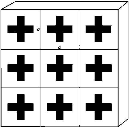
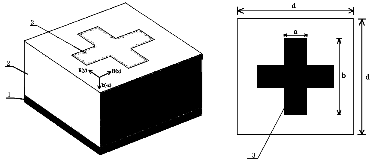
[0025] A terahertz double-band absorber based on a cross-shaped graphene material, with a structure such as Figure 1-3 As shown, it includes a metal reflection layer 1, a dielectric layer 2 and a pattern layer 3 arranged in sequence from bottom to top, and the metal reflection layer 1 is made of a metal material with high electrical conductivity (electric conductivity is 4.7×10 7 S / m) made of metal thin film, the thickness of the metal reflective layer 1 is 200 μm, and the metal material is gold; the dielectric constant of the dielectric layer 2 is 3.9, and the thickness of the dielectric layer 2 is 3.3 μm, and the dielectric layer 2 is a silicon dioxide film; the pattern layer 3 is composed of periodically arranged cross-shaped material structural units, the thickness of the pattern layer 3 is 1nm, and each cross-shaped material structural unit is composed of mutually perpendicular horizontal bands and The vertical bands are connected, the horizontal bands and the vertical b...

Embodiment 2

[0029] A terahertz double-band absorber based on a cross-shaped graphene material, with a structure such as Figure 1-3 As shown, it includes a metal reflection layer 1, a dielectric layer 2 and a pattern layer 3 arranged in sequence from bottom to top. The metal reflection layer 1 is a metal film made of a metal material with high conductivity. The metal reflection layer 1 The thickness is 230 μm, the metal material is silver; the dielectric constant of the dielectric layer 2 is 3.9, the thickness of the dielectric layer 2 is 3 μm, and the dielectric layer 2 is a silicon dioxide film; the pattern layer 3 is arranged periodically Composed of cross-shaped material structural units, the thickness of the pattern layer 3 is 1nm, each cross-shaped material structural unit is composed of mutually perpendicular horizontal bands and vertical bands connected, and the horizontal bands and vertical bands are made of graphene, The lattice period d of the cross-shaped material structure un...

Embodiment 3

[0032] A terahertz double-band absorber based on a cross-shaped graphene material, with a structure such as Figure 1-2 As shown, it includes a metal reflection layer 1, a dielectric layer 2 and a pattern layer 3 arranged in sequence from bottom to top. The metal reflection layer 1 is a metal film made of a metal material with high conductivity. The metal reflection layer 1 The thickness is 250 μm, the metal material is aluminum; the dielectric constant of the dielectric layer 2 is 3.9, the thickness of the dielectric layer 2 is 5 μm, and the dielectric layer 2 is a silicon dioxide film; the pattern layer 3 is arranged periodically Composed of cross-shaped material structural units, the thickness of the pattern layer 3 is 1nm, each cross-shaped material structural unit is composed of mutually perpendicular horizontal bands and vertical bands connected, and the horizontal bands and vertical bands are made of graphene, The lattice period d of the cross-shaped material structure ...


PUM

PropertyMeasurementUnit
Thicknessaaaaaaaaaa
Thicknessaaaaaaaaaa
Thicknessaaaaaaaaaa

Abstract

The invention discloses a terahertz double-waveband absorber based on a cross-shaped graphene material. The terahertz double-waveband absorber comprises a metal reflective layer, a dielectric layer and a pattern layer which are arranged in order from bottom to top. The pattern layer is formed by periodically arranged cross-shaped material structure units. Each cross-shaped material structure unitis composed of connected horizontal and vertical strips that perpendicular to each other. The horizontal and the vertical strips are made of graphene. The lattice period d of the cross-shaped materialstructure units is 3 to 5 [mu]m, and each horizontal strip and each vertical strip have a width a of 0.6 to 1 [mu]m and a length b is 1.2 to 2 [mu]m. Also provided is an application thereof. The absorber of the invention has a simple structure, does not require multi-layer material stacking or multiple resonators, is easy to integrate and high in stability, has special electromagnetic response, and has the characteristics of high absorption rate, high sensitivity, and flexible regulation.

Description

technical field [0001] The invention belongs to the technical field of metamaterials and electromagnetic functions, and in particular relates to a terahertz double-band absorber based on a cross-shaped graphene material and its application. Background technique [0002] Terahertz waves usually refer to electromagnetic waves with a frequency in the range of 0.1THz to 10THz. From the perspective of frequency, this band is located between millimeter waves and infrared rays, and belongs to the far-infrared band; from the perspective of energy, it is between electrons and photons. For a long time, due to the lack of research results and data on the terahertz wave band, people have little understanding of this wave, resulting in the formation of the phenomenon of "terahertz blank". Because terahertz waves are in a special region where electronics transitions to photonics, terahertz waves have many unique properties, such as broadband, transient, low energy, coherence, and so on. ...

Claims


Application Information

Patent Timeline
IPC IPC(8): G02B5/00H01Q17/00
CPCG02B5/003H01Q17/00
Inventor 范春珍田雨宸
Owner ZHENGZHOU UNIV
Why Eureka
Try Eureka