A terahertz double-band absorber based on cross-shaped graphene material and its application
A cross-shaped, graphene technology, used in instruments, antennas, optics, etc., can solve problems such as hindering potential applications and complex structures, and achieve the effects of easy integration, simple graphic structure, and good stability.
- Summary
- Abstract
- Description
- Claims
- Application Information
AI Technical Summary
Problems solved by technology
Method used
Image
Examples
Embodiment 1
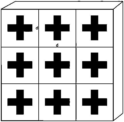
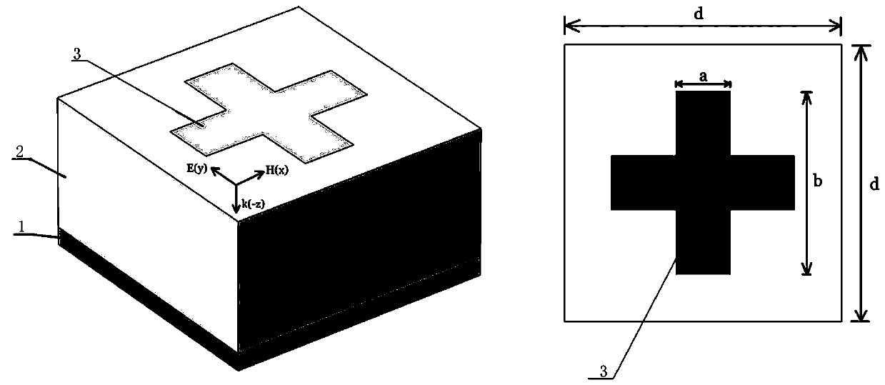
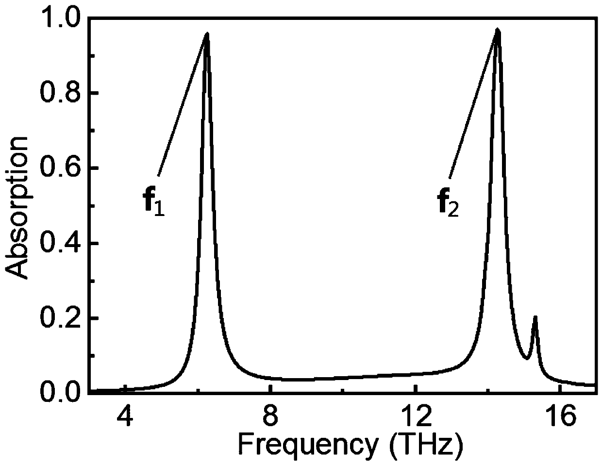
[0025] A terahertz double-band absorber based on a cross-shaped graphene material, with a structure such as Figure 1-3 As shown, it includes a metal reflection layer 1, a dielectric layer 2 and a pattern layer 3 arranged in sequence from bottom to top, and the metal reflection layer 1 is made of a metal material with high conductivity (conductivity is 4.7×10 7 S / m) made of metal thin film, the thickness of the metal reflective layer 1 is 200 μm, and the metal material is gold; the dielectric constant of the dielectric layer 2 is 3.9, and the thickness of the dielectric layer 2 is 3.3 μm, and the dielectric layer 2 is a silicon dioxide film; the pattern layer 3 is composed of periodically arranged cross-shaped material structural units, the thickness of the pattern layer 3 is 1nm, and each cross-shaped material structural unit is composed of mutually perpendicular horizontal bands and The vertical bands are connected, the horizontal bands and the vertical bands are made of gra...
Embodiment 2
[0029] A terahertz double-band absorber based on a cross-shaped graphene material, with a structure such as Figure 1-3 As shown, it includes a metal reflection layer 1, a dielectric layer 2 and a pattern layer 3 arranged in sequence from bottom to top. The metal reflection layer 1 is a metal film made of a metal material with high conductivity. The metal reflection layer 1 The thickness is 230 μm, the metal material is silver; the dielectric constant of the dielectric layer 2 is 3.9, the thickness of the dielectric layer 2 is 3 μm, and the dielectric layer 2 is a silicon dioxide film; the pattern layer 3 is arranged periodically Composed of cross-shaped material structural units, the thickness of the pattern layer 3 is 1nm, each cross-shaped material structural unit is composed of mutually perpendicular horizontal bands and vertical bands connected, and the horizontal bands and vertical bands are made of graphene, The lattice period d of the cross-shaped material structure un...
Embodiment 3
[0032] A terahertz double-band absorber based on a cross-shaped graphene material, with a structure such as Figure 1-2 As shown, it includes a metal reflection layer 1, a dielectric layer 2 and a pattern layer 3 arranged in sequence from bottom to top. The metal reflection layer 1 is a metal film made of a metal material with high conductivity. The metal reflection layer 1 The thickness is 250 μm, the metal material is aluminum; the dielectric constant of the dielectric layer 2 is 3.9, the thickness of the dielectric layer 2 is 5 μm, and the dielectric layer 2 is a silicon dioxide film; the pattern layer 3 is arranged periodically Composed of cross-shaped material structural units, the thickness of the pattern layer 3 is 1nm, each cross-shaped material structural unit is composed of mutually perpendicular horizontal bands and vertical bands connected, and the horizontal bands and vertical bands are made of graphene, The lattice period d of the cross-shaped material structure ...
PUM
| Property | Measurement | Unit |
|---|---|---|
| thickness | aaaaa | aaaaa |
| thickness | aaaaa | aaaaa |
| thickness | aaaaa | aaaaa |
Abstract
Description
Claims
Application Information


