Composite silicon hemisphere/graphene broadband terahertz metamaterial absorber
A metamaterial, graphene technology, applied in the direction of instruments, optics, electrical components, etc., can solve problems such as limiting absorption performance
- Summary
- Abstract
- Description
- Claims
- Application Information
AI Technical Summary
Problems solved by technology
Method used
Image
Examples
Embodiment Construction
[0015] The technical solution of the present invention will be further described below in conjunction with the examples, but it is not limited thereto. Any modification or equivalent replacement of the technical solution of the present invention without departing from the spirit and scope of the technical solution of the present invention should be covered by the technical solution of the present invention. in the scope of protection.
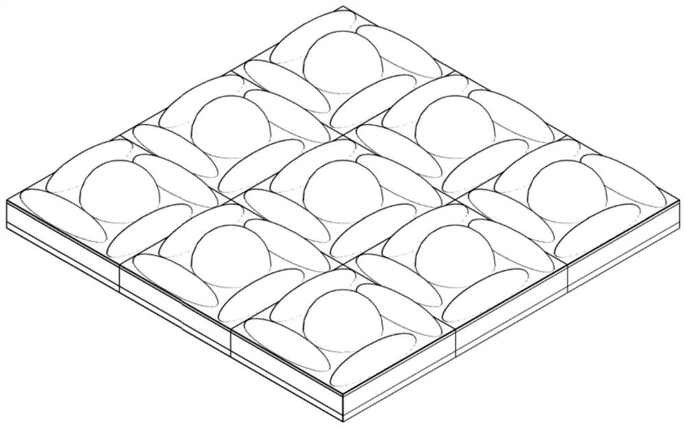
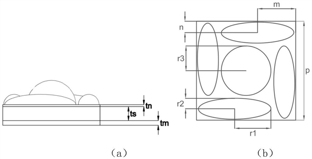
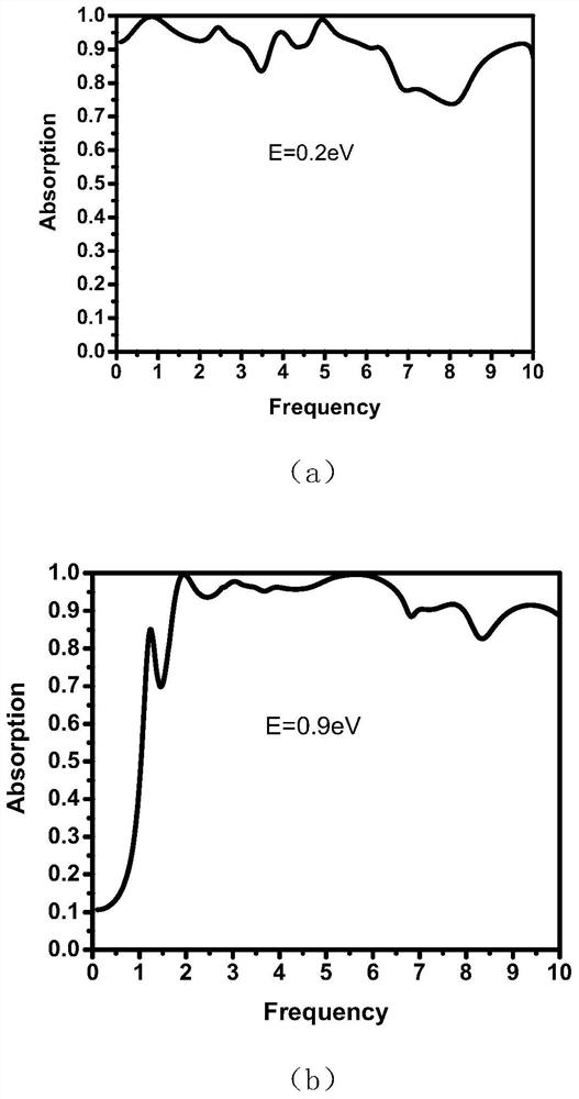
[0016] A composite silicon hemisphere / graphene based broadband terahertz metamaterial absorber, as figure 1 , 2 As shown, it includes metal reflective layer, dielectric layer, graphene layer and silicon hemisphere layer. The metal reflective layer is a continuous metal gold film with a conductivity of 4.561×10 7 S / m, its thickness tm=2 μm; Dielectric layer is polydimethylsiloxane (PDMS) thin film film, relative permittivity and loss tangent are 1.72 and 0.15, medium thickness ts=15 μm; Graphene layer chemical potential E=0.2eV and 0.9eV, thi...
PUM
| Property | Measurement | Unit |
|---|---|---|
| Thickness | aaaaa | aaaaa |
| Thickness | aaaaa | aaaaa |
| Thickness | aaaaa | aaaaa |
Abstract
Description
Claims
Application Information


