
GOA circuit

A circuit and capacitor technology, applied in the display field, to reduce current stress, avoid voltage difference, and improve quality

Active Publication Date: 2018-04-24
WUHAN CHINA STAR OPTOELECTRONICS TECH CO LTD
View PDF7 Cites 20 Cited by
  • Summary
  • Abstract
  • Description
  • Claims
  • Application Information

AI Technical Summary

Problems solved by technology

[0006] The existing GOA circuit includes cascaded multi-level GOA units. Each level of GOA unit includes a pull-up control module, an output module and a pull-down module. The output module has a first N-type thin film transistor, and its gate is electrically connected to the The first node of the multi-level GOA unit, the source is connected to the clock signal, and the drain is electrically connected to the output terminal of the level GOA unit. When working, within one frame, the pull-up control module of the multi-level GOA unit sequentially The potential of the first node of the level GOA unit becomes a high potential and maintains it for a period of time, correspondingly turning on the first N-type thin film transistor in the output module of the multilevel GOA unit for a period of time, and the clock signal lasts for a period of time The square wave of the output pulse, so the drain of the first N-type thin film transistor outputs the scan signal corresponding to the clock signal in the moment when the first N-type thin film transistor of the output module of the multi-level GOA unit is turned on, and then the multi-level GOA unit The pull-down module sequentially pulls down the potential of the first node of the multi-level GOA unit and the potential of the output terminal, and keeps the low potential by the pull-down maintenance module to realize the progressive output of scanning signals. However, in the above-mentioned GOA circuit, in the time of one frame Inside, the output terminal of the multi-level GOA unit, that is, the drain of the first N-type thin film transistor in the output module is at a low potential for a long time, and the source is at a low potential due to the access to the pulse square wave clock signal. The time of high potential and low potential is half of the length of one frame, so that the first N-type thin film transistor in the output module has a voltage difference between the source and drain for a long time to generate current stress (stress). The electrical condition of the first N-type thin film transistor in the output module will be affected, which will affect the normal switching, and then affect the normal operation of the GOA circuit, resulting in abnormal display on the display panel and reducing product quality.

Method used


Image

  • GOA circuit
  • GOA circuit
  • GOA circuit

Examples


no. 1 example

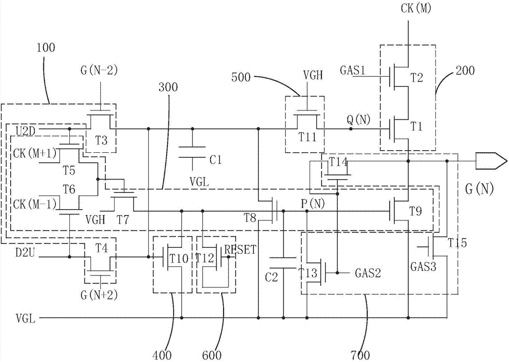
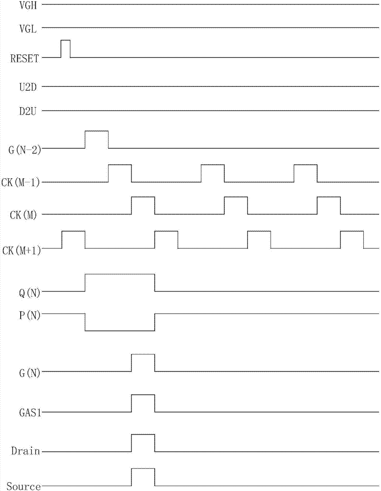
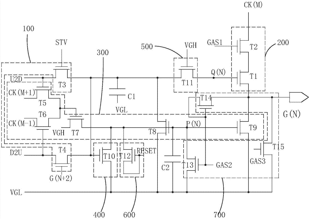
[0044] see Figure 1 to Figure 4 , the first embodiment of a GOA circuit provided by the present invention, the first embodiment of the GOA circuit of the present invention includes cascaded multi-level GOA units, and each level of GOA units includes: a forward and reverse scanning control module 100 , the output module 200, the pull-down module 300 and the first capacitor C1.

[0045] see figure 1 , assuming that N and M are positive integers, except for the first level, second level, penultimate level and last level of GOA units, in the N level GOA unit:

[0046] The forward and reverse scan control module 100 accesses the forward scan signal U2D and the reverse scan signal D2U, and is electrically connected to the output terminal G(N-2) of the N-2th level GOA unit, the N+2th level GOA The output terminal G(N+2) of the unit and the first node Q(N) are used for the output of the N+2th level GOA unit according to the potential of the output terminal G(N-2) of the N-2th level...


PUM


Abstract

The invention provides a GOA circuit. According to the GOA circuit, a second thin film transistor is arranged in an output module, the drain electrode of the second thin film transistor is electrically connected with the source electrode of a first thin film transistor, a first control signal is accessed to the grid electrode of the second thin film transistor, an Mth clock signal is accessed to the source electrode of the second thin film transistor, and opening and closure of the second thin film transistor are controlled through the first control signal; or the drain electrode of the secondthin film transistor is electrically connected with the source electrode of the first thin film transistor, the Mth clock signal is accessed to the grid electrode of the second thin film transistor,the source electrode of the second thin film transistor is electrically connected with a first node, and then the second thin film transistor is communicated when the Mth clock signal is at a high level and the first node is at a high level, and is cut off at other moments. Therefore, a voltage difference between the source electrode and the drain electrode of the first thin film transistor is avoided, the current stress to the first thin film transistor is reduced, and the product quality is effectively improved.

Description

technical field [0001] The invention relates to the field of display technology, in particular to a GOA circuit. Background technique [0002] A Liquid Crystal Display (LCD) has many advantages such as a thin body, power saving, and no radiation, and has been widely used. Such as: LCD TV, mobile phone, personal digital assistant (PDA), digital camera, computer screen or notebook computer screen, etc., occupy a dominant position in the field of flat panel display. [0003] Most of the liquid crystal displays currently on the market are backlight liquid crystal displays, which include a liquid crystal display panel and a backlight module. The working principle of the liquid crystal display panel is to pour liquid crystal molecules between the thin film transistor array substrate (ThinFilm Transistor Array Substrate, TFT Array Substrate) and the color filter substrate (ColorFilter, CF), and apply a driving voltage on the two substrates to Control the rotation direction of the...

Claims


Application Information

Patent Timeline
Patent Type & Authority Applications(China)
IPC IPC(8): G09G3/36
CPCG09G3/3677G09G3/3696G09G3/20G09G2300/0408G09G2310/0286G11C19/28G09G2310/062G09G2310/08
Inventor 洪光辉
Owner WUHAN CHINA STAR OPTOELECTRONICS TECH CO LTD
Learn More