Manufacturing method of buried word line

A manufacturing method and word line technology, applied in semiconductor/solid-state device manufacturing, electrical components, transistors, etc.

Active Publication Date: 2018-04-27
UNITED MICROELECTRONICS CORP +1
View PDF6 Cites 6 Cited by
  • Summary
  • Abstract
  • Description
  • Claims
  • Application Information

AI Technical Summary

Problems solved by technology

However, there is still a lot of room for improvement in the structure design and channel control of general vertical transistors, which is the goal of active research in this field

Method used


Image

  • Manufacturing method of buried word line
  • Manufacturing method of buried word line
  • Manufacturing method of buried word line

Examples


Embodiment Construction

[0040] In order to enable those who are familiar with the technical field of the present invention to further understand the present invention, the preferred embodiments of the present invention are listed below, together with the accompanying drawings, to describe in detail the composition of the present invention and the desired effects .

[0041] For the convenience of description, the drawings of the present invention are only schematic diagrams for easier understanding of the present invention, and the detailed proportions thereof can be adjusted according to design requirements. As for the up-down relationship of the relative components in the figures described in the text, those skilled in the art should understand that they refer to the relative positions of the objects, so all of them can be reversed to present the same components, which should all be disclosed in this specification. The range is described here.

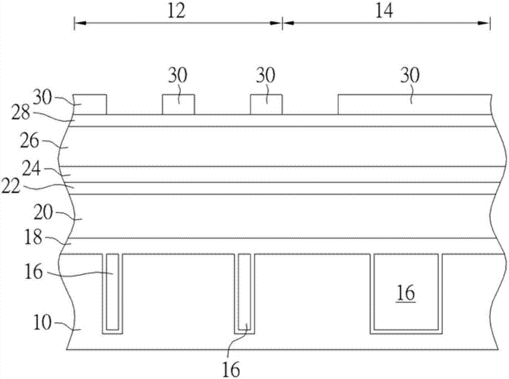
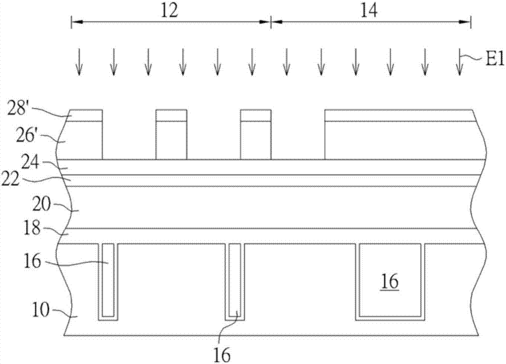
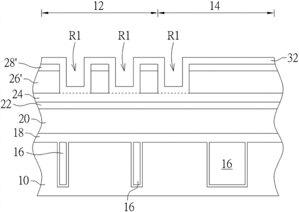
[0042] Figure 1-Figure 11 A schematic cross-sectiona...


PUM


Abstract

The invention discloses a manufacturing method of a buried word line. The manufacturing method comprises the steps of providing a substrate firstly, wherein the substrate comprises a plurality of shallow trench isolation parts; next, forming a plurality of first patterned material layers which are positioned above the substrate, wherein a first groove is included between any two adjacent first patterned material layers; next, forming at least one second patterned material layer which is positioned in the first groove; by taking each first patterned material layer and the second patterned material layer as a mask layer, performing a first etching step; and forming a plurality of second grooves at least in the shallow trench isolation parts and the substrate.

Description

technical field [0001] The invention relates to the field of semiconductor manufacturing technology, in particular to a method for manufacturing an embedded character line. Background technique [0002] Dynamic random access memory (dynamic random access memory, DRAM) is a kind of volatile memory, which is composed of a plurality of storage units. Each memory cell is mainly composed of a transistor and a capacitor controlled by the transistor, and each memory cell is electrically connected to each other through a word line (WL) and a bit line (BL). [0003] In order to increase the density of dynamic random access memory (DRAM) to speed up the operation speed of components, and to meet consumer demand for miniaturized electronic devices, the length of the channel region of transistors in dynamic random access memory (DRAM) will have a continuous shortening trend. However, in this way, the transistor will suffer from serious short channel effects, as well as problems such a...

Claims


Application Information

Patent Timeline
Patent Type & Authority Applications(China)
IPC IPC(8): H01L21/8242H01L27/108
CPCH10B12/01H10B12/00H10B12/48H10B12/482H10B12/488
Inventor 陈立强李甫哲郭明峰陈界得朱贤士
Owner UNITED MICROELECTRONICS CORP
Why Eureka
Try Eureka