Supercharge Your Innovation With Domain-Expert AI Agents!

Production method of a 3D NAND wire hole including silicon-rich silicon nitride isolating dielectric layer

A silicon silicon nitride layer and silicon-rich silicon nitride technology, applied in semiconductor devices, electrical components, electrical solid devices, etc., can solve the problems of poor step coverage of SiN layer, large etching energy, affecting the electrical performance of devices, etc. Achieve the effect of improving stability and reliability and avoiding uneven distribution

Active Publication Date: 2018-05-04
YANGTZE MEMORY TECH CO LTD
View PDF3 Cites 0 Cited by
  • Summary
  • Abstract
  • Description
  • Claims
  • Application Information

AI Technical Summary

Problems solved by technology

[0005] The above-mentioned silicon nitride layer can protect the silicon on the side wall of the wire hole and the tungsten metal on the bottom layer during pickling, and can prevent the wire hole from expanding due to pickling corrosion. However, NH is generally used when growing silicon nitride according to the traditional process. 3 gas, while due to heavy metals on NH 3 The decomposition has a catalytic effect, and there may be heavy metals W and NH 3 Therefore, the step coverage of the formed SiN layer will be poor, and it will affect the resistance of the wire
This will cause the problem of uneven thickness of the upper and lower silicon nitride layers in the wire hole, as shown in Figure 4. Figure 4(a)-4(c) They are the SiN layer surveying drawings of the upper, middle and bottom of the wire hole respectively. As can be seen from the figure, the thickness of the SiN layer formed as the wire hole goes down becomes thicker, and the thickness of the SiN layer at the bottom of the wire hole is nearly twice the thickness of the top
The above-mentioned thickness distribution of the SiN layer has a certain influence on the subsequent etching of SiN at the bottom of the wire hole, so that the etching of the SiN layer requires more energy or time, and due to the high hardness of SiN, in step 3 (c) The etching energy required to open the deposited SiN at the bottom is relatively large, which will increase the probability of excessive etching, so that the metal W at the bottom will be damaged, which will bring certain stability and reliability to the process. difficulty
according to Figure 5 The energy dispersive spectroscopy (EDS) map shown after bottom etching shows that the SiN layer prepared by the prior art will have obvious nitrogen residues after bottom etching
and Image 6 Then it shows the lead hole after over-etching, such as Image 6 The wire hole shown in the dotted box, due to over-etch, can cause wire connection errors and affect the electrical performance of the device

Method used


Image

  • Production method of a 3D NAND wire hole including silicon-rich silicon nitride isolating dielectric layer
  • Production method of a 3D NAND wire hole including silicon-rich silicon nitride isolating dielectric layer
  • Production method of a 3D NAND wire hole including silicon-rich silicon nitride isolating dielectric layer

Examples


Embodiment Construction

[0028] Exemplary embodiments of the present disclosure will be described in more detail below with reference to the accompanying drawings. Although exemplary embodiments of the present disclosure are shown in the drawings, it should be understood that the present disclosure may be embodied in various forms and should not be limited by the embodiments set forth herein. Rather, these embodiments are provided for more thorough understanding of the present disclosure and to fully convey the scope of the present disclosure to those skilled in the art.

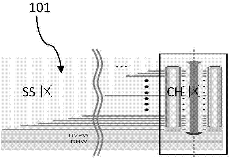
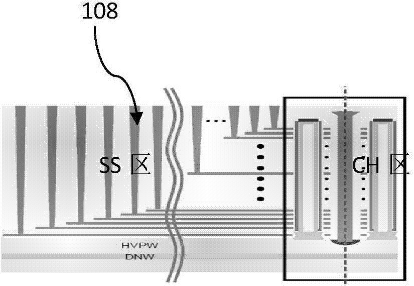
[0029] The technological process of the metal tungsten plug in the SS region of the present invention is the same as the aforementioned Figure 3(a)-3(d) The shown prior art process flow is similar, the difference is that the aforementioned silicon nitride layer is replaced by a silicon-rich silicon nitride layer, and the specific process flow is as follows Figure 7(a)-7(e) It includes the following steps: first, as shown in Figur...


PUM


Abstract

Provided is a production method of a 3D NAND wire hole. The wire hole is formed in a string selection region and is filled with tungsten to allow wire connection; before a pre-cleaning step, a silicon-rich silicon nitride layer is deposited in the wire hole to serve as an isolating dielectric layer. In the production method, the silicon-rich silicon nitride deposition process is used to replace traditional silicon nitride deposition, so that top-bottom non-uniformity of the isolating dielectric layer in the wire hole caused by NH3 decomposition or reaction is relieved; therefore, etching problem caused by the distribution non-uniformity of the isolating dielectric layer is avoided, and process stability and reliability are improved.

Description

technical field [0001] The present application relates to the technical field of three-dimensional (3D) memory, and more specifically, relates to a preparation method of a 3D NAND wiring hole including a silicon-rich silicon nitride isolation dielectric layer. Background technique [0002] With the rapid development of flash memory, the structure of 3D flash memory has been developed rapidly, and NAND flash memory is a better storage device than hard disk drives. As people pursue non-volatile storage products with low power consumption, light weight and good performance , 3D NAND flash memory has been widely used in electronic products. [0003] In the 3D NAND structure, in the current process, a plurality of wire holes are formed by multiple etching in the SS (string selection) region, and metal tungsten is filled in the wire holes by chemical vapor deposition (CVD), so as to realize wire connection, Figure 1(a) and 1(b) Schematic diagrams of wire holes and tungsten wire...

Claims


Application Information

Patent Timeline
Patent Type & Authority Applications(China)
IPC IPC(8): H01L27/11524H01L27/11529H01L27/11551H10B41/35H10B41/20H10B41/41
CPCH10B41/35H10B41/41H10B41/20
Inventor 郭帅吴俊王家友朱峰李春龙
Owner YANGTZE MEMORY TECH CO LTD
Features
  • R&D
  • Intellectual Property
  • Life Sciences
  • Materials
  • Tech Scout
  • Unparalleled Data Quality
  • Higher Quality Content
  • 60% Fewer Hallucinations
Learn More