
A multi-camera module

A multi-camera and module technology, used in image communication, radiation control devices, TVs, etc., can solve the problems of the large overall volume of the COB packaging process module and the high manufacturing cost of the camera module, and achieve low investment in production line equipment and manufacturing. Low cost and volume reduction effect

Active Publication Date: 2020-07-31
TRULY OPTO ELECTRONICS
View PDF5 Cites 0 Cited by
  • Summary
  • Abstract
  • Description
  • Claims
  • Application Information

AI Technical Summary

Problems solved by technology

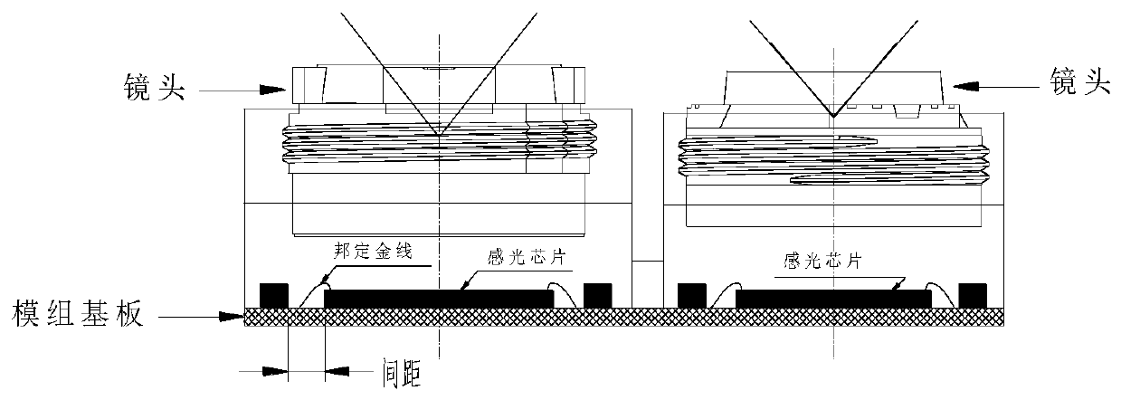
The photosensitive chip is connected to the multi-camera module by bonding gold wires, and a certain distance needs to be designed with other components of the module. Please refer to figure 1 As shown, the distance between capacitors and other devices and COB chips is larger than that of CSP chips, and the overall volume of COB packaging process modules will be larger than that of CSP process modules; and COB packaging process is used to manufacture modules, and COB bonding gold wire equipment needs to be invested. Each piece of equipment is at the million-level level, and the establishment of a COB process production line requires huge capital investment, and the manufacturing cost of camera modules is relatively high

Method used


Image

  • A multi-camera module
  • A multi-camera module
  • A multi-camera module

Examples


Embodiment Construction

[0042] In order to enable those skilled in the art to better understand the solution of the present invention, the present invention will be further described in detail below in conjunction with the accompanying drawings and specific embodiments. Apparently, the described embodiments are only some of the embodiments of the present invention, but not all of them. Based on the embodiments of the present invention, all other embodiments obtained by persons of ordinary skill in the art without making creative efforts belong to the protection scope of the present invention.

[0043] The terms "first", "second", "third" and "fourth" in the description of the present application and the above drawings are used to distinguish different objects, rather than to describe a specific order. Furthermore, the terms "comprising" and "having", and any variations thereof, are intended to cover a non-exclusive inclusion. For example, a process, method, system, product, or device comprising a se...


PUM

PropertyMeasurementUnit
sizeaaaaaaaaaa

Abstract

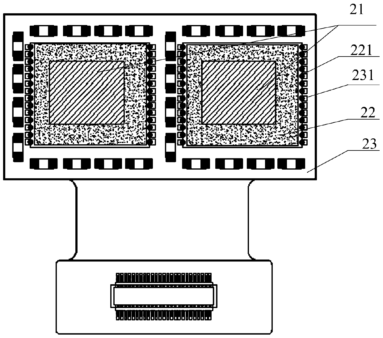
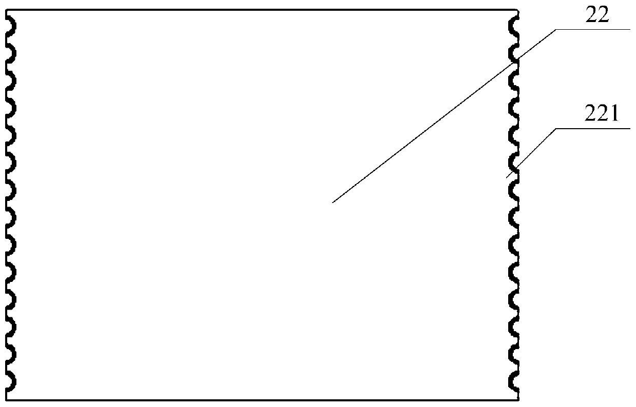
The embodiment of the invention discloses a multi-camera module, which includes a bare chip, a packaging substrate and a module substrate. The outer side of the packaging substrate is provided with side pads, and solder material is provided on the side pads; the peripheral size of the packaging substrate is larger than the size of the bare chip, and the size difference between the packaging substrate and the bare chip does not exceed the preset Threshold; the bare chip is set on the packaging substrate, and the functional pins of the bare chip are connected to the side pads using the semiconductor lead process to form a packaged chip; the packaged chip is mounted on the surface of the module substrate and soldered through the side of the packaged chip The pads are connected to the solder pads of the module substrate. The image effect of the multi-camera module prepared by this application is equivalent to that of the module produced by the COB packaging process, but it avoids the use of bonding gold wires in the traditional COB packaging process, and the investment in production line equipment is less, and the manufacturing cost is lower; The size of the entire multi-camera module is conducive to the development of the multi-camera module toward miniaturization.

Description

technical field [0001] Embodiments of the present invention relate to the technical field of packaging photographic equipment, in particular to a multi-camera module. Background technique [0002] As users have higher and higher requirements for the quality of imaging pictures, the continuous development of camera and photography equipment technology is required to obtain high-quality and high-definition pictures. [0003] The optical quality of the lens and the size of the sensor determine the imaging quality of the camera, and with the light and thin requirements of camera equipment (such as mobile terminals), the sensor size and the optical quality of the lens are limited. Moreover, the pixels of a single camera face a bottleneck when developing to a higher level, and it is impossible to obtain high-quality pictures by increasing the pixels. For example, for mobile phone cameras, 20 million pixels have reached the limit. In addition, users do not need mobile phones to ac...

Claims


Application Information

Patent Timeline
Patent Type & Authority Patents(China)
IPC IPC(8): H01L27/146H04N5/225
CPCH01L27/14601H01L27/14625H01L27/14687H04N23/50H04N23/55
Inventor 韦有兴
Owner TRULY OPTO ELECTRONICS
Learn More